Maxcntx, Basex – Cirrus Logic EP93xx User Manual
Page 423
DS785UM1
10-29
Copyright 2007 Cirrus Logic
DMA Controller
EP93xx User’s Guide
1
0
1
0
10
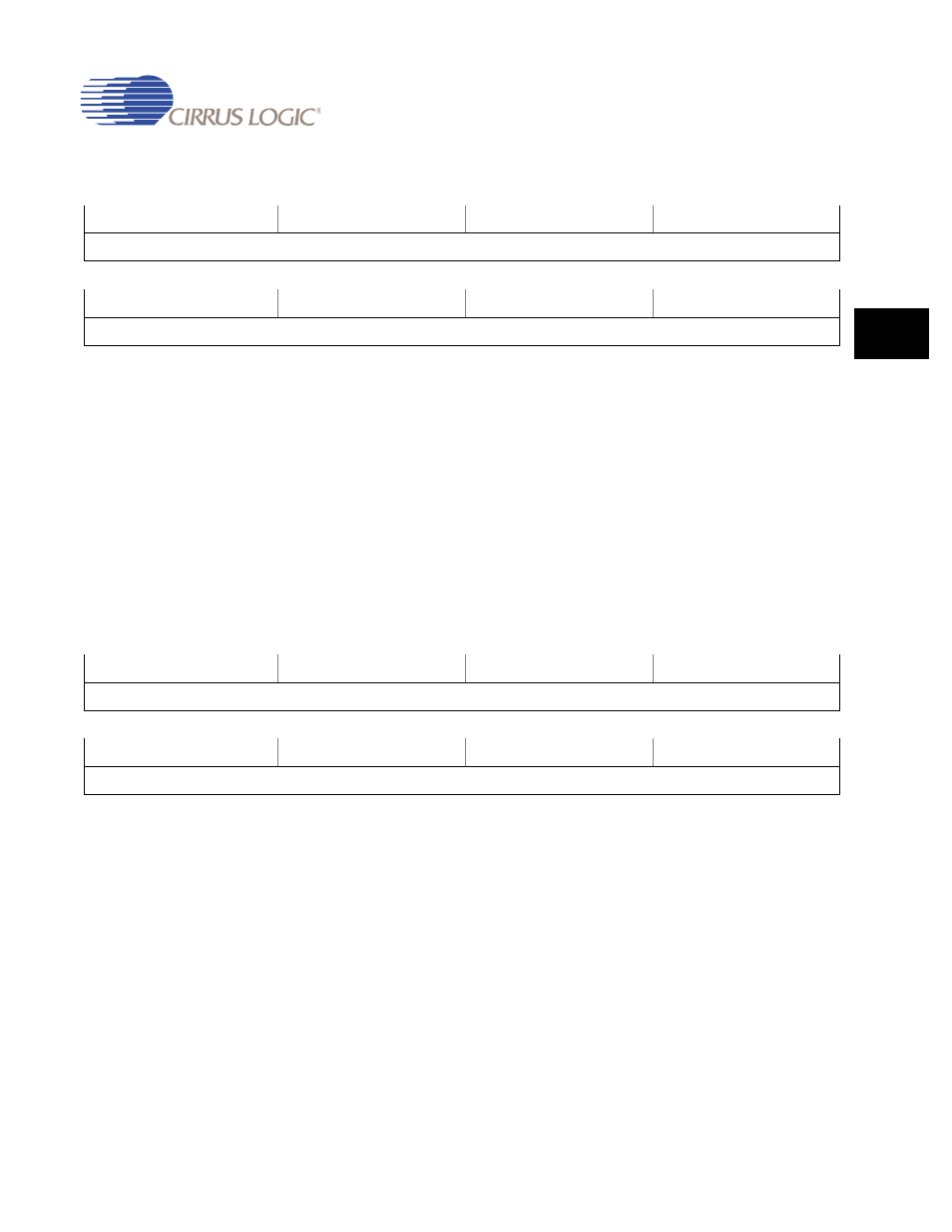
MAXCNTx
Address:
MAXCNT0: Channel Base Address + 0x0020 - Read/Write
MAXCNT1: Channel Base Address + 0x0030 - Read/Write
Definition:
x = “0” or “1”. Maximum byte count for the buffer. Represents the double buffer
per channel. Only the low order 16 bits are used. Each MAXCNTx register
must be programmed before it’s corresponding BASEx register.
Bit Descriptions:
RSVD:
Reserved. Unknown During Read.
MAXCNTx:
Maximum byte count for the buffer.
BASEx
Address:
BASE0: Channel Base Address + 0x0024 - Read/Write
BASE1: Channel Base Address + 0x0034 - Read/Write
Definition:
Base address for the current and next DMA transfer.
Bit Descriptions:
BASEx:
x = “0” or “1”. Base address for the current and next DMA
transfer. Loaded with start address after enabling the DMA
Channel, the latter event required to take the Channel
State machine into the STALL state, the former event
required to enter the ON State.
31
30
29
28
27
26
25
24
23
22
21
20
19
18
17
16
RSVD
15
14
13
12
11
10
9
8
7
6
5
4
3
2
1
0
MAXCNTx
31
30
29
28
27
26
25
24
23
22
21
20
19
18
17
16
BASEx
15
14
13
12
11
10
9
8
7
6
5
4
3
2
1
0
BASEx