4 24 bpp mode, 4 24 bpp mode -12 – Cirrus Logic EP93xx User Manual
Page 276
8-12
DS785UM1
Copyright 2007 Cirrus Logic
Graphics Accelerator
EP93xx User’s Guide
8
8
8
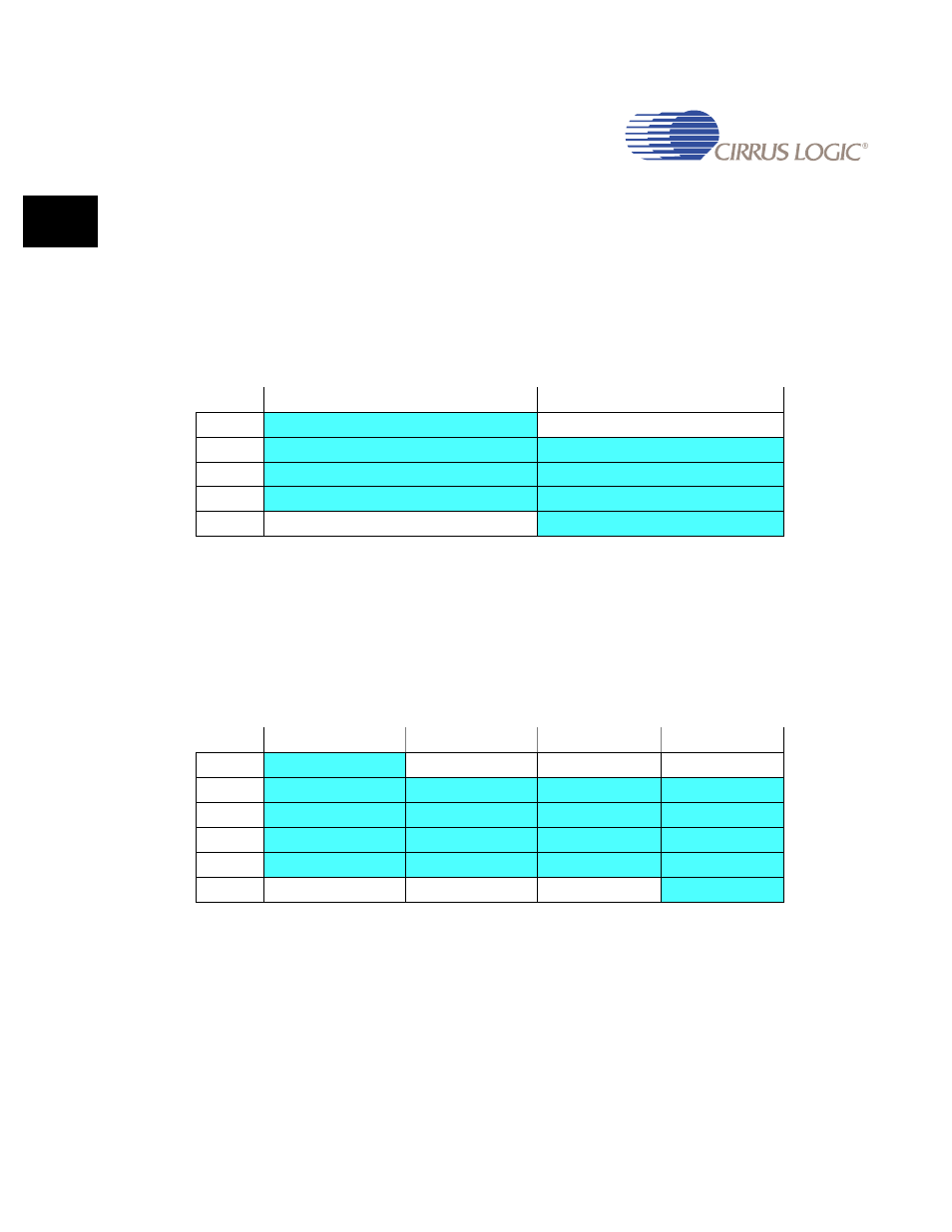
Let the starting SDRAM address of the destination image be 0x0044.
shows that
Pixel 0 starts at bit 16. The start pixel, P0, is in the word at address 0x0044 and has a
beginning bit position of 16. This makes 16 = 0x10 the value that is used for the SPEL field in
the
register.
The end pixel, P7, is in the word at address 0x0054 and has a beginning bit position of 0. This
makes 0 = 0x0 the value that is used for the EPEL field in the
register.
Note:The word count for this example would be: 5 - 1 = 4 words, since P7 ends in the 5th word.
So, WIDTH = 0x4 would be written to the
register.
8.5.2.4 24 BPP mode
This 24 BPP mode is the most difficult because, unlike the other modes, pixels will span
words. For a Block Copy where 6 pixels are transferred per scan line, let the starting SDRAM
address of the source image be 0x0000.
shows that Pixel 1 starts at bit 24. The
start pixel, P1, is in the word at address 0x0000 and has a beginning bit position of 24. This
makes 24 = 0x18 the value that is used for the SPEL field in the
register.
Let the starting SDRAM address of the destination image be 0x0058.
shows that
Pixel 1 starts at bit 24. The start pixel, P1, is in the word at address 0x0058 and has a
beginning bit position of 24. This makes 24 = 0x18 the value that is used for the SPEL field in
the
register.
The end pixel, P6, is in the word at address 0x006C and has a beginning bit position of 0.
This makes 0 = 0x0 the value that is used for the EPEL field in the
register.
Table 8-18. 16 BPP Memory Layout for Destination Image
Address
31
16
15
0
0x0044
P0
0x0048
P2
P1
0x004C
P4
P3
0x0050
P6
P5
0x0054
P7
Table 8-19. 24 BPP Memory Layout for Source Image
Address
31
24
23
16
15
8
7
0
0x0000
P1
P0
P0
P0
0x0004
P2
P2
P1
P1
0x0008
P3
P3
P3
P2
0x000C
P5
P4
P4
P4
0x0010
P6
P6
P5
P5
0x0014
P7
P7
P7
P6