2 i2s rx registers, Table 21-8. i, S rx registers – Cirrus Logic EP93xx User Manual
Page 675

DS785UM1
21-19
Copyright 2007 Cirrus Logic
I
2
S Controller
EP93xx User’s Guide
2
1
2
1
21
Definition:
TX2 Channel Enable
Bit Descriptions:
RSVD:
Reserved. Unknown During Read.
i2s_tx2_EN:
TX2 Channel Enable
21.7.2 I
2
S RX Registers
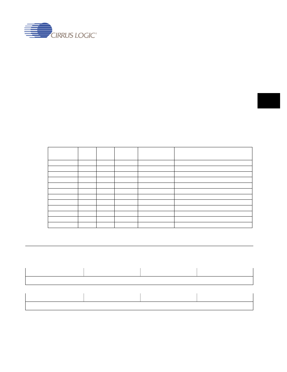
The following table summarizes the register set in the I
2
S Receiver block. Each of the
registers listed are addressable. The left and right data registers for channels 0, 1 and 2 can
be accessed by both APB and DMA accesses. The remaining registers are concerned with
control/status information and can be only accessed through the APB bus.
I
2
S RX Register Descriptions
I2SRX0Lft
Address:
0x8082_0040 - Read Only
Default:
Table 21-8. I
2
S RX Registers
Address
Type
Width
Reset
Value
Name
Description
0x8082_0040
R
32
0x0
I2SRX0Lft
Left Receive data register for channel 0
0x8082_0044
R
32
0x0
I2SRX0Rt
Right Receive data register for channel 0
0x8082_0048
R
32
0x0
I2SRX1Lft
Left Receive data register for channel 1
0x8082_004C
R
32
0x0
I2SRX1Rt
Right Receive data register for channel 1
0x8082_0050
R
32
0x0
I2SRX2Lft
Left Receive data register for channel 2
0x8082_0054
R
32
0x0
I2SRX2Rt
Right Receive data register for channel 2
0x8082_0058
R/W
2
0x0
I2SRXLinCtrlData
Line Control data register
0x8082_005C
R/W
2
0x0
I2SRXCtrl
Control register
0x8082_0060
R/W
2
0x0
I2SRXWrdLen
Word Length
0x8082_0064
R/W
1
0x0
I2SRX0En
RX0 Channel Enable
0x8082_0068
R/W
1
0x0
I2SRX1En
RX1 Channel Enable
0x8082_006C
R/W
1
0x0
I2SRX2En
RX2 Channel Enable
31
30
29
28
27
26
25
24
23
22
21
20
19
18
17
16
i2s_rx0_left
15
14
13
12
11
10
9
8
7
6
5
4
3
2
1
0
i2s_rx0_left
