2 address/data/control required by memory system – Cirrus Logic EP93xx User Manual
Page 506
13-10
DS785UM1
Copyright 2007 Cirrus Logic
SDRAM, SyncROM, and SyncFLASH Controller
EP93xx User’s Guide
1
3
1
3
13
13.8.2 Address/Data/Control Required by Memory System
An independent device configuration register,
,
,
, and
, is provided for each of the four
synchronous memory domains. Each domain can be configured for either an SDRAM,
SyncROM, or SyncFLASH device type. Only one device type can be configured per domain.
However, different domains can be configured for different device types.
Each of the four synchronous memory domains can be configured to be either 16- or 32-bits
wide and each will support 32-bit (word), 16-bit (half-word), and 8-bit (byte) accesses to or
from the synchronous memory device. If the external memory bus is 16-bits wide, two
external bus accesses are automatically made to Read or Write a 32-bit word. This is why a
burst-of-eight accesses is used to Read or Write devices that are attached to a 16-bit bus
while only a burst-of-four accesses is used to Read or Write devices that are attached to a
32-bit bus.
When writing to external memory, byte lane enable signals are output on the nDQM[3:0] pins,
where the DQMn0 pin controls the least-significant byte lane, the DQMn1 pin controls the
next to least-significant byte lane, the DQMn2 pin controls the next to most- significant byte
lane, and the DQMn3 pin controls the most-significant byte lane. The memory device uses
the byte lane enable signals on the DQMn pins to determine which byte lane data it should
accept during a Write operation. For example, if a 32-bit word is to be written to a memory
device on a 32-bit memory bus, DQMn[3:0] = ‘0000’ is output to alert the memory device that
it should accept Write data from all four byte lanes. However, if an 8-bit byte is to be written to
the next to least-significant byte of a memory device on a 32-bit bus, DQMn[3:0] = ‘1101’ is
output to alert the memory device that it should accept Write data from only the next to least-
significant byte lane and reject Write data from the other byte lanes. As another example, if a
32-bit word is to be written to a memory device on a 16-bit data bus, two 16-bit writes are
automatically performed to the memory device. For each 16-bit Write, DQM[1:0] = ‘00’ and
DQM[3:2] are not used.
shows a memory addressing example for a 256 Mbit synchronous memory
device with 13-row x 9-column x 2-bank addressing attached to a 16-bit memory bus. Note
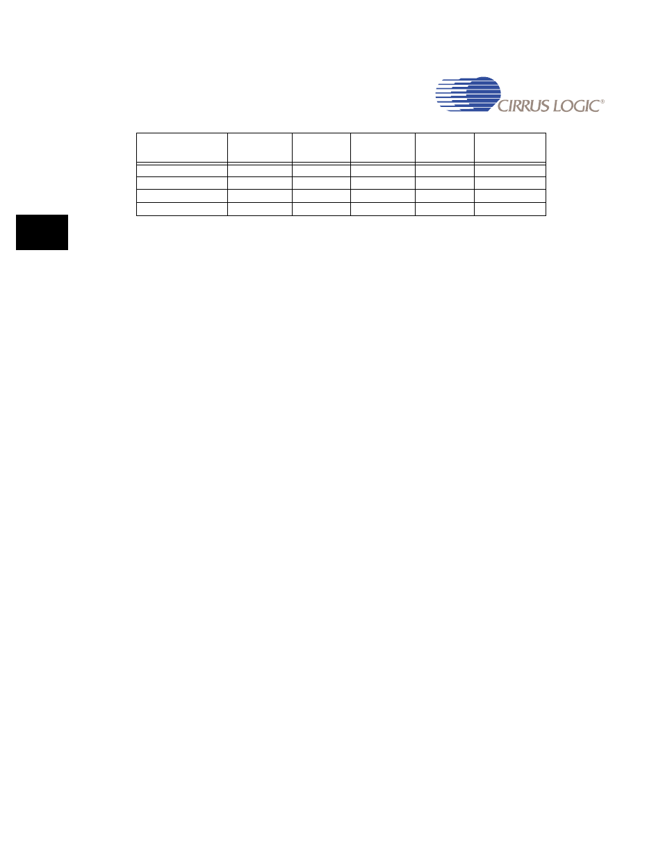
0
1
1
1
1
nSDCS3
X
1
1
1
0
nSDCS2
X
1
1
0
1
nSDCS1
X
1
1
0
0
nSDCS0
Table 13-9. Chip Select Decoding
Boot Option
(ASDO)
A31
A30
A29
A28
Chip select