Control – Cirrus Logic EP93xx User Manual
Page 416

10-22
DS785UM1
Copyright 2007 Cirrus Logic
DMA Controller
EP93xx User’s Guide
1
0
1
0
10
Register Descriptions
CONTROL
Address:
Channel Base Address + 0x0000 - Read/Write
Definition:
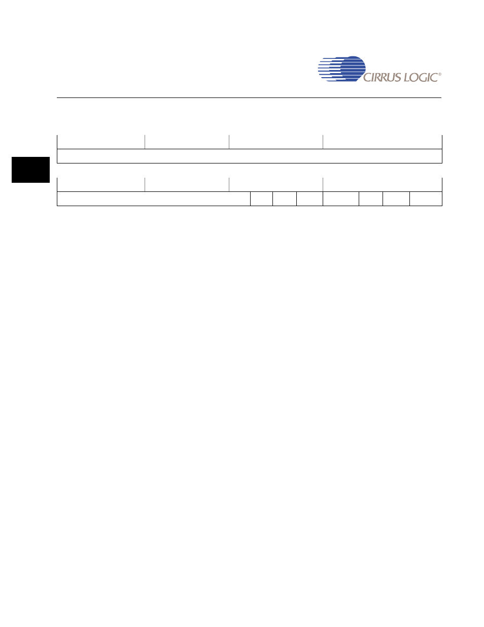
This is the Channel Control Register, used to configure the DMA Channel.
Important Programming Note: The control register should be read
immediately after being written. This action will allow hardware state machines
to transition and prevent a potential problem when the registers are being
written in back to back clock cycles.
Bit Descriptions:
RSVD:
Reserved. Unknown During Read.
STALLIntEn:
Setting this bit to 1 enables the generation of the STALL
interrupt in the STALL State of the DMA Channel State
machine. Setting this bit to zero disables generation of the
STALL Interrupt.
NFBIntEn:
Setting this bit to 1 enables the generation of the NFB
(next frame buffer) interrupt in the ON State of the DMA
Channel State machine. Setting this bit to zero disables
generation of the NFB Interrupt. Normally when the
channel is enabled, this bit should be 1. However in the
case where the current buffer is the last, then this bit can
be cleared to prevent the generation of an interrupt while
the DMA State machine is in the ON State.
ChErrorIntEn:
Setting this bit to 1 enables the ChError Interrupt which
indicates if the buffer transfer occurred with an error.
ENABLE:
Setting this bit to 1 enables the channel, clearing this bit
disables channel, and causes the remaining
unpacker/packer data to be discarded. The channel must
always be enabled before writing the Base address
register.
31
30
29
28
27
26
25
24
23
22
21
20
19
18
17
16
RSVD
15
14
13
12
11
10
9
8
7
6
5
4
3
2
1
0
RSVD
ICE
ABORT
ENABLE
ChErrorIntEn
RSVD
NFBIntEn
STALLIntEn
