9 registers, 9 registers -17, Table 13-12. address bits used for chip select -17 – Cirrus Logic EP93xx User Manual
Page 513
DS785UM1
13-17
Copyright 2007 Cirrus Logic
SDRAM, SyncROM, and SyncFLASH Controller
EP93xx User’s Guide
1
3
1
3
13
13.9 Registers
The Synchronous Memory controller has seven registers as shown in
Configuration registers allow software to specify the operating parameters of the
Synchronous Memory controller according to the memory device types being used. The
Refresh Timer register allows software to specify the time period between successive
synchronous memory refresh commands. The Boot Status allows software to determine the
state of the boot configuration pins.
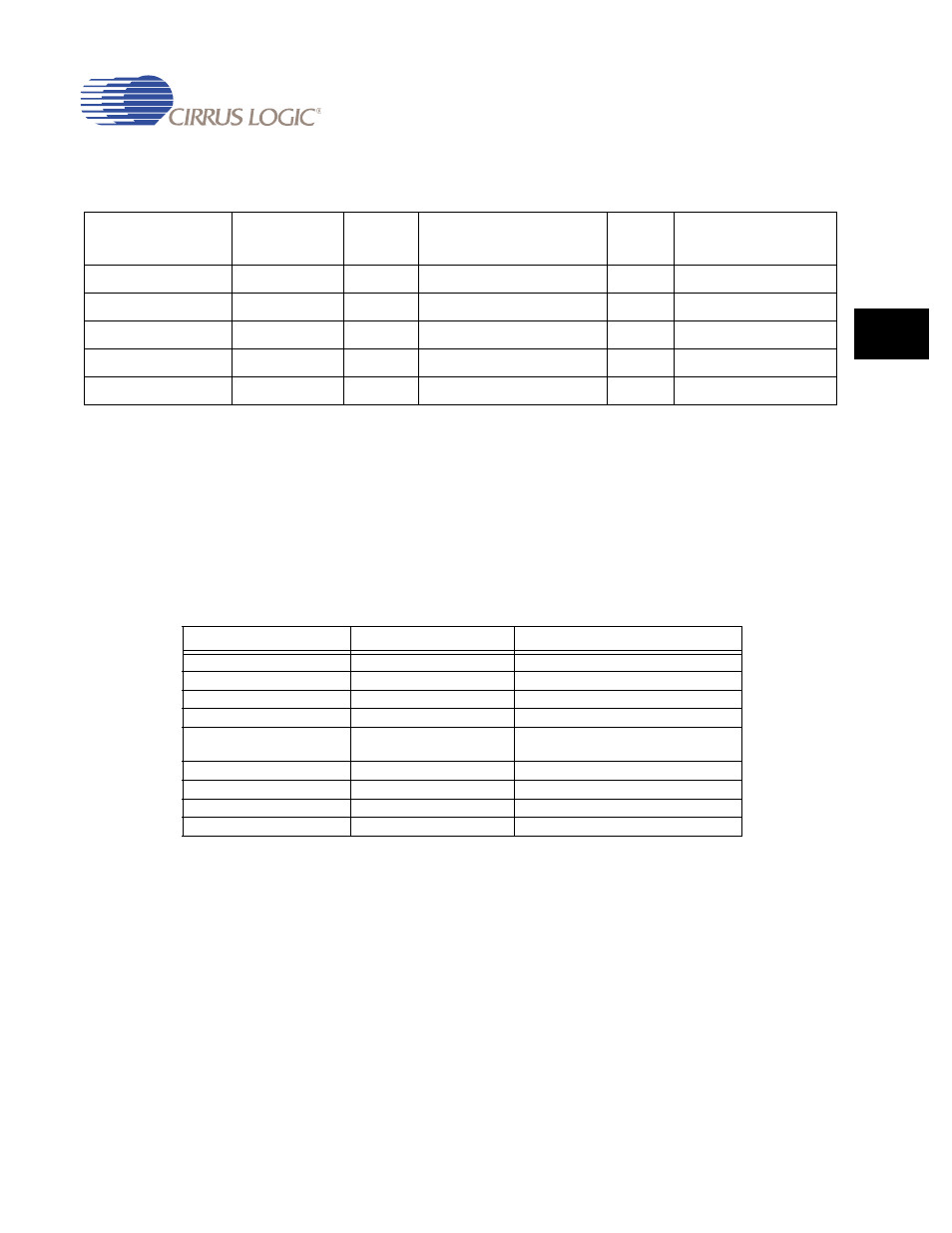
Table 13-12. Address Bits Used for Chip Select
Boot Option
(ASDO)
A31 A30
A29
A28 Chip
select
1 0
0 0 0
nSDCS3
0 1
1 1 1
nSDCS3
X 1
1 1 0
nSDCS2
X 1
1 0 1
nSDCS1
X 1
1 0 0
nSDCS0
Table 13-13. Synchronous Memory Controller Registers
Address
Name
Description
0x8006_0000
Reserved
0x8006_0004
Global Configuration
0x8006_0008
Refresh Timer
0x8006_000C
Boot Configuration Pins Status
(See Below)
0x8006_0010
Synchronous Device Configuration 0
0x8006_0014
Synchronous Device Configuration 1
0x8006_0018
Synchronous Device Configuration 2
0x8006_001C
Synchronous Device Configuration 3