3 registers, 3 registers -10, Table 27-6. ide interface register map -10 – Cirrus Logic EP93xx User Manual
Page 780
27-10
DS785UM1
Copyright 2007 Cirrus Logic
IDE Interface
EP93xx User’s Guide
2
7
2
7
27
For both PIO and MDMA modes, the actual throughput is limited by the ARM Core's ability to
service requests, not raw bandwidth. For UDMA, the throughput is dependent on the
bandwidth available to the DMA controller.
27.3 Registers
Register Descriptions
IDECtrl
Address:
0x800A_0000 - Read/Write
Default:
0x0000_0063
Definition:
IDE Control Register. This register is used for IDE PIO control operations.
IORDY, INTRQ, DMARQ, and DASPn reflect external pins. Their reset state
can vary depending on system implementation and system configuration.
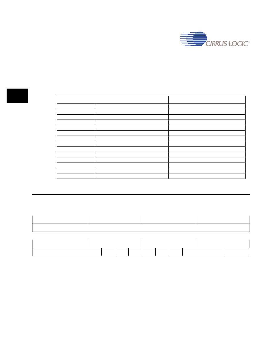
Table 27-6. IDE Interface Register Map
Address Name
Description
0x800A_0000
IDECtrl
IDE Control Register
0x800A_0004
IDECfg
IDE Configuration Register
0x800A_0008
IDEMDMAOp
IDE MDMA Operation Register
0x800A_000C
IDEUDMAOp
IDE UDMA Operation Register
0x800A_0010
IDEDataOut
IDE PIO Data Output Register
0x800A_0014
IDEDataIn
IDE PIO Data Input Register
0x800A_0018
IDEMDMADataOut
IDE MDMA Data Output Register
0x800A_001C
IDEMDMADataIn
IDE MDMA Data Input Register
0x800A_0020
IDEUDMADataOut
IDE UDMA Data Output Register
0x800A_0024
IDEUDMADataIn
IDE UDMA Data Input Register
0x800A_0028
IDEUDMASts
IDE UDMA Status Register
0x800A_002C
IDEUDMADebug
IDE UDMA Debug Register
0x800A_0030
IDEUDMAWrBufSts
IDE UDMA Write Buffer Status Register
0x800A_0034
IDEUDMARdBufSts
IDE UDMA Read Buffer Status Register
31
30
29
28
27
26
25
24
23
22
21
20
19
18
17
16
RSVD
15
14
13
12
11
10
9
8
7
6
5
4
3
2
1
0
RSVD
IORDY
INTRQ
DMARQ
DASPn
DIOWn
DIORn
DA
CS1n
CS0n