Clkset1, E) to, Stfclr – Cirrus Logic EP93xx User Manual
Page 144: Rsvd: there are no readable bits in this register

5-18
DS785UM1
Copyright 2007 Cirrus Logic
System Controller
EP93xx User’s Guide
5
5
5
STFClr
Address:
0x8093_001C - Write
Definition:
Writing to the STFClr location will clear the CLDFLG, WDTFLG and RSTFLG
in the register,
. Any data written to the register triggers
the clearing.
Bit Descriptions:
RSVD:
There are no readable bits in this register.
ClkSet1
Address:
0x8093_0020 - Read/Write
Definition:
The ClkSet1 system control register is one of two register that control clock
speeds.
Note: When a write is performed to the ClkSet1 location, it must be immediately followed by 5
NOP instructions. This is needed to flush the instruction pipeline in the ARM920T core.
Writing to this register will cause the the device to enter Standby for between 8 ms to
16 ms. Reading from this register will not cause an entry into Standby mode.
Bit Descriptions:
RSVD:
Reserved. Unknown During Read.
PLL1_X2IPD:
These 5 register bits set the input divider for PLL1
operation. On power-on-reset the value is set to 00111b (7
decimal).
Note: The value in the register is the actual coefficient minus one.
31
30
29
28
27
26
25
24
23
22
21
20
19
18
17
16
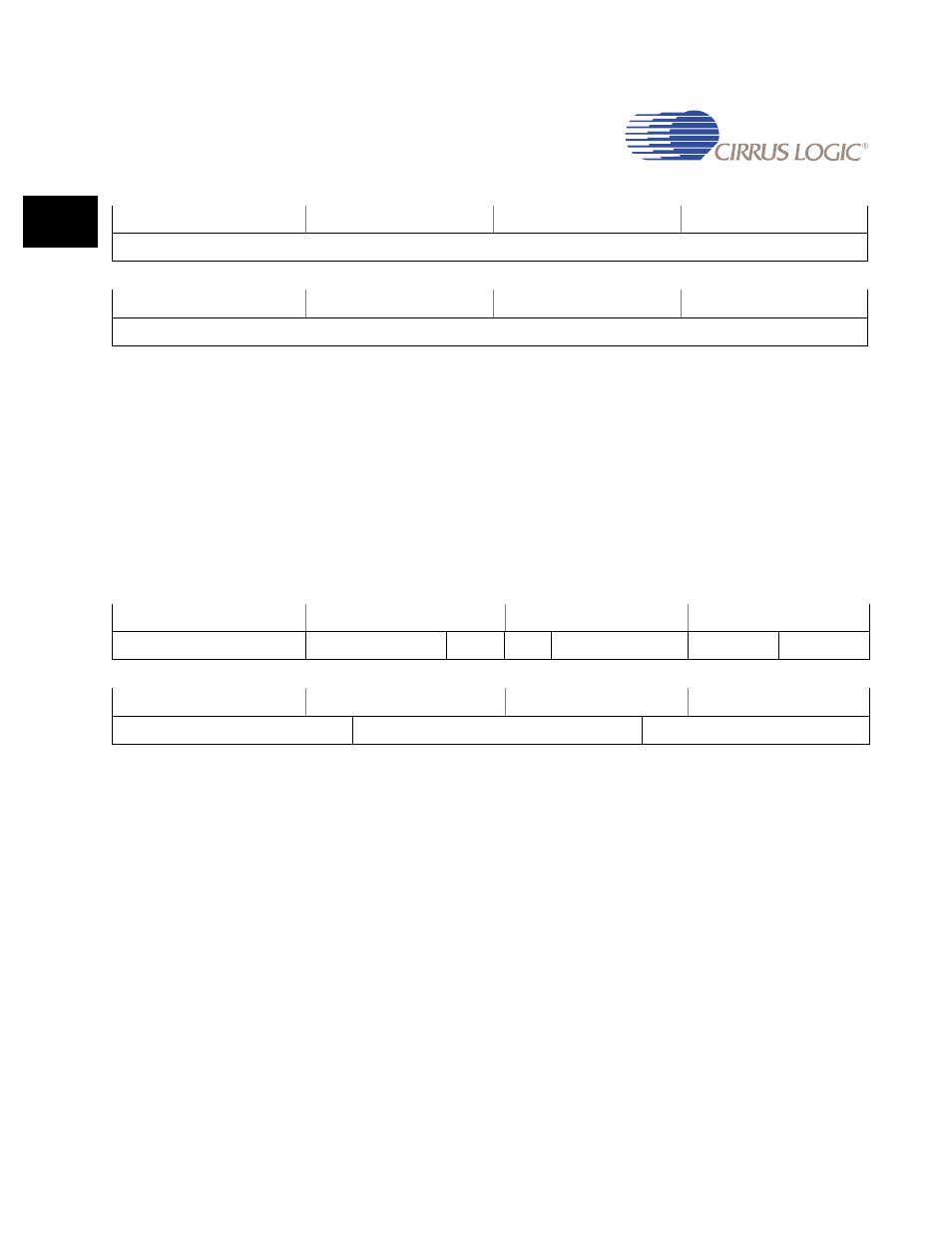
RSVD
15
14
13
12
11
10
9
8
7
6
5
4
3
2
1
0
RSVD
31
30
29
28
27
26
25
24
23
22
21
20
19
18
17
16
RSVD
FCLK DIV
SMC ROM
nBYP1
HCLK DIV
PCLK DIV
PLL1_PS
15
14
13
12
11
10
9
8
7
6
5
4
3
2
1
0
PLL1 X1FBD1
PLL1 X2FBD2
PLL1 X2IPD
