Cirrus Logic EP93xx User Manual
Page 196
D
S
7
85U
M
1
7-1
4
C
o
pyr
ig
h
t 20
07
C
ir
ru
s
Lo
gic
Rast
er Engi
ne W
ith Ana
log/
LCD Inte
grate
d
Tim
ing
and
Inte
rf
a
c
e
EP93
xx U
ser
’s
G
u
ide
77
7
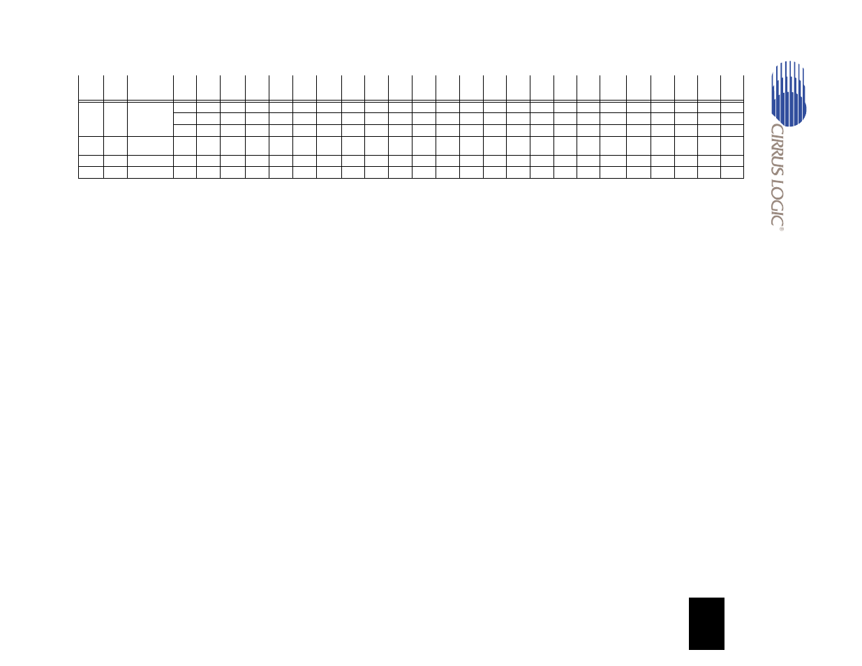
*These bits are an ORed combination of the bit value shown and the next significant bit below (This rounds the color value to nearest
color).
**These bits do not get a substitute and are defined to the values controlled by the pixel output mode in the upper part of the table.
0x6
0x0
0x8
dual 2 2/3
pixels per
clock
X
X
X
X
X
X
X
X
L G2
L B2
L R1
L G1
L B1
L R0
L G0
L B0 U G2 U B2
U R1
U G1 U B1 U R0 U G0 U B0
X
X
X
X
X
X
X
X
L B5
L R4
L G4
L B4
L R3
L G3
L B3
L R2 U B5 U R4
U G4
U B4
U R3 U G3 U B3 U R2
X
X
X
X
X
X
X
X
L R7
L G7
L B7
L R6
L G6
L B6
L R5
L G5 U R7 U G7
U B7
U R6 U G6 U B6 U R5 U G5
**
**
CCIREN
subs
**
**
**
**
**
**
**
**
**
**
**
**
**
**
**
**
D(7)
D(6)
D(5)
D(4)
D(3)
D(2)
D(1)
D(0)
**
**
LCDEN subs
**
**
**
**
**
**
**
XECL YSCL
**
**
**
**
**
**
**
**
**
**
**
**
**
**
**
**
**
ACEN subs
**
**
**
**
**
**
AC
**
**
**
**
**
**
**
**
**
**
**
**
**
**
**
**
**
Table 7-3. Output Pixel Transfer Modes (Continued)
Shift
Mode
Color
Mode
Output
Mode
P(23) P(22) P(21) P(20) P(19) P(18) P(17) P(16) P(15) P(14) P(13) P(12) P(11) P(10) P(9) P(8) P(7) P(6)
P(5)
P(4) P(3) P(2) P(1) P(0)