Cirrus Logic EP93xx User Manual
Page 501
DS785UM1
13-5
Copyright 2007 Cirrus Logic
SDRAM, SyncROM, and SyncFLASH Controller
EP93xx User’s Guide
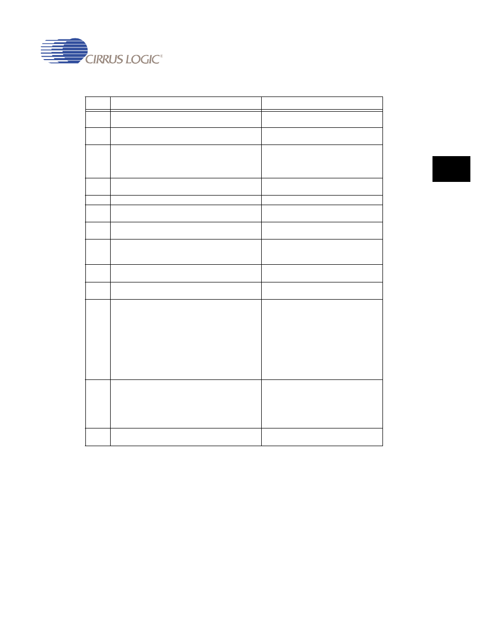
1
3
1
3
13
2
Write a ‘1’ or ‘0’ to the External Bus Width bit in the
appropriate
register
‘1’ specifies 16-bit memory bus width
‘0’ specifies 32-bit memory bus width
3
Write Initialize = ‘0’, MRS = ‘1’, and LCR = ‘0’ to the
register
To allow the Mode register inside the
external SDRAM device to be accessed
4
Read from the external SDRAM’s Mode register
with Row and Bank address = 0x2 or 0x3 (see
SDRAM data sheet)
0x2 -- Burst Length = 4 (32-bit wide
memory bus)
0x3 -- Burst Length = 8 (16-bit wide
memory bus)
5
Write Initialize = ‘1’, MRS = ‘1’, and LCR = ‘0’ to the
register
To issue continuous NOP accesses
6
Wait 200
μ
s
SDRAM requirement
7
Write Initialize = ‘1’, MRS = ‘0’, and LCR = ‘0’ to the
register
To issue a Pre-Charge All accesses
8
Write Refcnt = 0xB into the
register
To provide a refresh every 10 SDCLK
cycles
9
Wait for at least 80 SDCLK cycles
To provide 8 refresh cycles to all
SDRAMs in
space
10
Write the normal operating value to the Refcnt field
in the
register
To establish normal refresh operation
11
Write Initialize = ‘0’, MRS = ‘1’, and LCR = ‘0’ to the
register
To allow the Mode register inside the
SDRAM device to be accessed
12
Perform a read from each SDRAM in the
space. The value of the
address that is read defines the value that is
written into the Mode register (see SDRAM device
datasheet). The address value is dependent on the
configuration of the memory system since the
actual SDRAM address pins are mapped
differently onto the processor’s address pins for
16- and 32-bit wide memory systems. (This is the
reason for step 2).
To set up the Mode register inside each
SDRAM device
13
Write parameters corresponding to those
programmed into the SDRAM devices Mode
register into the corresponding fields of the
register. Write other fields in
register as appropriate
for the given SDRAM usage.
To initialize the SDRAM controller timing
14
Write Initialize = ‘0’, MRS = ‘0’, and LCR = ‘0’ to the
register.
To start normal operation
Table 13-4. General SDRAM Initialization Sequence
Step
Action
Reason