1 diagrams and state machines, 1 diagrams and state machines -2, Figure 27-1. ide interface signal connections -2 – Cirrus Logic EP93xx User Manual
Page 772
27-2
DS785UM1
Copyright 2007 Cirrus Logic
IDE Interface
EP93xx User’s Guide
2
7
2
7
27
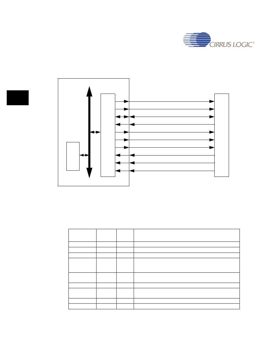
27.2.1 Diagrams and State Machines
Figure 27-1. IDE Interface Signal Connections
Table 27-1. IDE Host to IDE Interface Definition
IDE Pin
Type
No. of
Pins
Description
CS0n
-
1
Chip select for device registers with base address 0x1F0
CS1n
-
1
Chip select for device registers with base address 0x3F0
DA[2:0]
-
3
3-bit binary encoded address
DIORn/
HDMARDYn/
HSTROBE
-
1
Strobe signal to read device regs or data port/
Flow control signal for Ultra DMA data-in burst/
Flow control signal for Ultra DMA data-out burst
DIOWn/
STOP
-
1
Strobe signal to write device regs or data port/
Terminates an Ultra DMA burst
DMACKn
-
1
DMA acknowledge to DMARQ to initiate DMA transfers
DASPn GPIO
1
Signal to indicate that a device is active, or that Device 1 is
present
DMARQ
GPIO
1
DMA request for DMA to and from the controller
INTRQ INT
1
Device
interrupt
CS0n, CS1n
DA[2:0]
DD[15:0]
DMARQ
DMACKn
DIORn/HDMARDYn/HSTROBE
DIOWn/STOP
INTRQ
IORDY/DDMARDYn/DSTROBE
IDE Controller
IDE Connector
DMA
AHB Bus
Processor
Controller
DASPn