2 i2s transmitter channel overview, Table 21-1. i, Table 21-2. audio interfaces pin assignment -2 – Cirrus Logic EP93xx User Manual
Page 658: Table 21-1, S transmitter channel overview
21-2
DS785UM1
Copyright 2007 Cirrus Logic
I
2
S Controller
EP93xx User’s Guide
2
1
2
1
21
The primary I
2
S port and the I
2
S clocks are multiplexed and can be assigned to either the
SSP pins or the Ac97 pins. The second and third I
2
S ports use the same clock pins as the
primary I
2
S port, but their serial output and input pins are multiplexed with EGPIO pins. The
second I
2
S port's serial output and serial input pins are multiplexed with EGPIO[4] and
EGPIO[5] respectively and are enabled by setting DeviceCfg.A1onG. The third I
2
S port's
serial output and serial input pins are multiplexed with EGPIO[6] and EGPIO[13] respectively
and are enabled by setting DeviceCfg.A2onG.
21.2 I
2
S Transmitter Channel Overview
Each I
2
S TX channel provides a single stereo I
2
S compliant output. The Transmit channel
can operate in master or slave mode. Data is transferred between the ARM Core and the I
2
S
controller via an interrupt based mechanism or DMA access. The ARM Core or host
processor must write words in multiples of 2 (that is, a left and right stereo pair). These words
are serially shifted out, timed with respect to the audio bit clock and word clock (SCLK and
LRCK) that are generated (see
for additional details).
The key features of the I
2
S transmitter are:
•
Three transmit data channels, master or slave mode.
Table 21-1. I
2
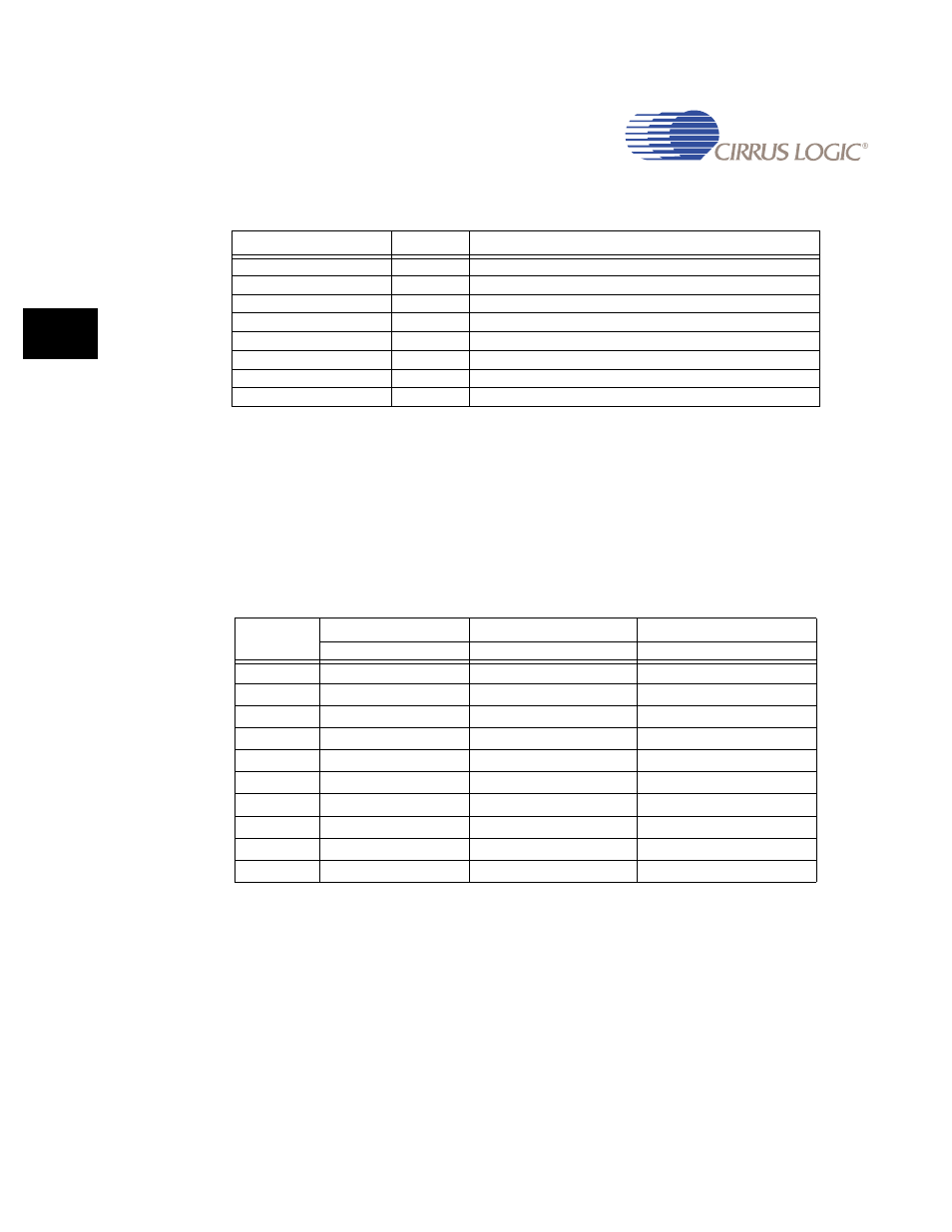
S Controller Input and Output Signals
Signal Name
Type
Description
lrck
IN
Left/right Word Audio slave clock.
sck
IN
Audio bit slave clock.
sdi0
IN
Serial data for channel 0
sdi1
IN
Serial data for channel 1
sdi2
IN
Serial data for channel 2
sdo0
OUT
Serial data output for TX channel 0
sdo1
OUT
Serial data output for TX channel 1
sdo2
OUT
Serial data output for TX channel 2
Table 21-2. Audio Interfaces Pin Assignment
Pin
Name
Normal Mode
I
2
S on SSP Mode
I
2
S on AC'97 Mode
Pin Description
Pin Description
Pin Description
SCLK1
SPI Bit Clock
I
2
S Serial Clock
SPI Bit Clock
SFRM1
SPI Frame Clock
I
2
S Frame Clock
SPI Frame Clock
SSPRX1
SPI Serial Input
I
2
S Serial Input
SPI Serial Input
SSPTX1
SPI Serial Output
I
2
S Serial Output
SPI Serial Output
(No I
2
S Master Clock)
ARSTn
AC'97 Reset
AC'97 Reset
I
2
S Master Clock
ABITCLK
AC'97 Bit Clock
AC'97 Bit Clock
I
2
S Serial Clock
ASYNC
AC'97 Frame Clock
AC'97 Frame Clock
I
2
S Frame Clock
ASDI
AC'97 Serial Input
AC'97 Serial Input
I
2
S Serial Input
ASDO
AC'97 Serial Output
AC'97 Serial Output
I
2
S Serial Output