Cirrus Logic EP93xx User Manual
Page 703
DS785UM1
22-15
Copyright 2007 Cirrus Logic
AC’97 Controller
EP93xx User’s Guide
2
2
2
2
22
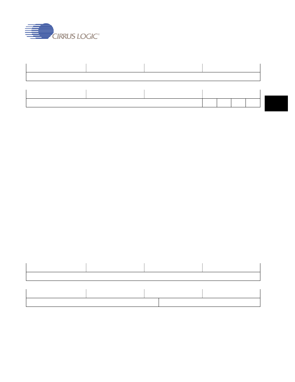
AC97IEx
Address:
AC97IE1 - 0x8088_0018 - Read/Write
AC97IE2 - 0x8088_0038 - Read/Write
AC97IE3 - 0x8088_0058 - Read/Write
AC97IE4 - 0x8088_0078 - Read/Write
Definition:
Interrupt Enable Register. The AC97IE registers control the Interrupt Enables
for the FIFOs within the controller. All bits are cleared on reset.
Bit Descriptions:
RSVD:
Reserved. Unknown During Read.
RIE:
Receive Interrupt Enable - If this bit is set to “1”, the FIFO
receive interrupt is enabled.
TIE:
Transmit Interrupt Enable - If this bit is set to “1”, the FIFO
transmit interrupt is enabled.
RTIE:
Receive Timeout Interrupt Enable - If this bit is set to “1”,
the FIFO receive timeout interrupt is enabled.
TCIE:
Transmit Complete Interrupt Enable - If this bit is set to “1”,
the FIFO transmit complete interrupt is enabled.
AC97S1Data
Address:
0x8088_0080 - Read/Write
Definition:
Slot 1 Data Register. The AC97S1Data register is a read / write register. When
a write has occurred to this register, the data contained within it is sent on the
31
30
29
28
27
26
25
24
23
22
21
20
19
18
17
16
RSVD
15
14
13
12
11
10
9
8
7
6
5
4
3
2
1
0
RSVD
RIE
TIE
RTIE
TCIE
31
30
29
28
27
26
25
24
23
22
21
20
19
18
17
16
RSVD
15
14
13
12
11
10
9
8
7
6
5
4
3
2
1
0
RSVD
DATA