Devicecfg – Cirrus Logic EP93xx User Manual
Page 151
DS785UM1
5-25
Copyright 2007 Cirrus Logic
System Controller
EP93xx User’s Guide
5
5
5
DeviceCfg
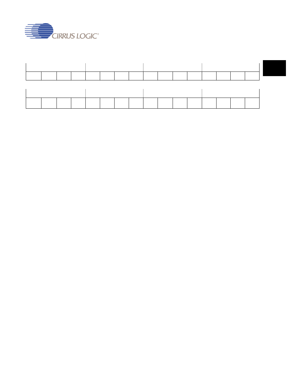
Address:
0x8093_0080 - Read/Write, Software locked
Default:
0x0000_0000
Definition:
Device Configuration Register. This register controls the operation of major
system functions.
Bit Descriptions:
RSVD:
Reserved. Unknown During Read.
0:
This bit must be written as “0”.
SHena:
Standby/Halt enable. When 1, allows the system to enter
Standby or Halt on a read from the Standby and Halt
registers, respectively.
KEYS:
Key matrix inactive.
1 - Key Matrix controller inactive,
0 - Key Matrix controller active.
ADCPD:
ADC Power Down.
1 - ADC and clocks are powered down.
0 - ADC and clocks are active. ADCPD must be zero for
normal touch screen operation and for direct ADC
operation.
RAS:
Raster inactive.
1 - Disables video pixel clock to most of the Raster engine,
0 - Normal video clock to Raster engine.
RasOnP3:
Raster On SDRAM Port 3.
1 - The Raster video refresh SDRAM accesses use the
system primary AHB to get video data.
0 - Raster video refresh uses the private AHB on SDRAM
Port 0.
31
30
29
28
27
26
25
24
23
22
21
20
19
18
17
16
SWRST
D1onG
D0onG
IonU2
GonK
TonG
MonG
U3EN
CPENA
A2onG
A1onG
U2EN
EXVC
U1EN
TIN
RSVD
15
14
13
12
11
10
9
8
7
6
5
4
3
2
1
0
HC3IN
HC3EN
HC1IN
HC1EN
HonIDE
GonIDE
PonG
EonIDE
I2Son
SSP
I2Son
AC97
0
RASOn
P3
RAS
ADCPD
KEYS
SHena