3 external reference frequency setup, Figure 9-25 on, Atmega128rfa1 – Rainbow Electronics ATmega128RFA1 User Manual
Page 81
81
8266A-MCU Wireless-12/09
ATmega128RFA1
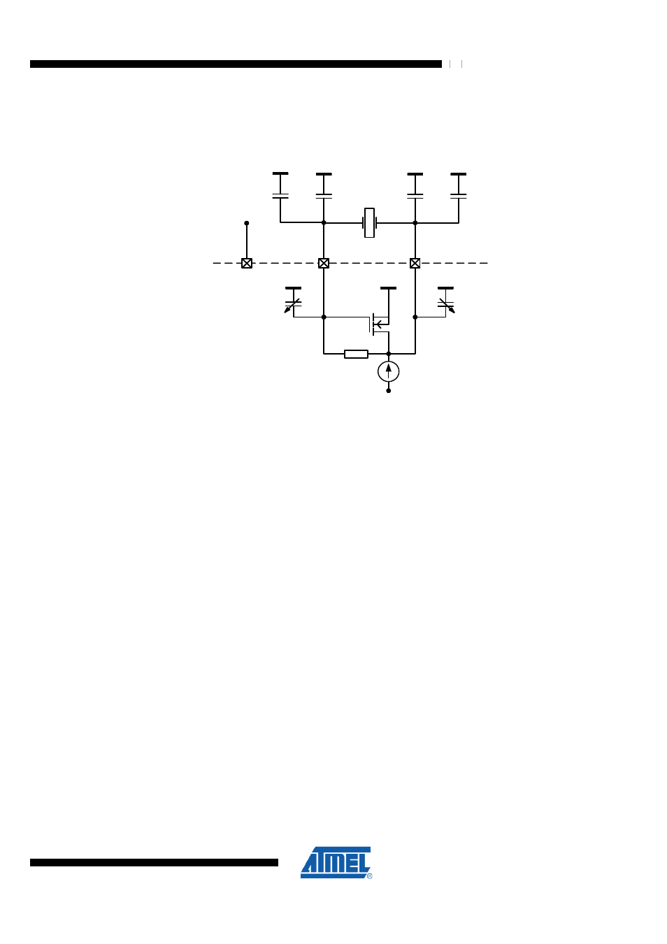
The following figure shows all parasitic capacitances, such as PCB stray capacitances
and the pin input capacitance summarized to C
PAR
.
Figure 9-25. Simplified XOSC Schematic with External Components
CX
CX
16MHz
XTAL2
XTAL1
EVDD
C
TRIM
C
TRIM
C
PAR
C
PAR
IC internal
PCB
XTAL_TRIM[3:0]
EVDD
V
EVDD
XTAL_TRIM[3:0]
Additional internal trimming capacitors C
TRIM
are available. Any value in the range from
0 pF to 4.5 pF with a 0.3 pF resolution is selectable using XTAL_TRIM of register
XOSC_CTRL. To calculate the total load capacitance, the following formula can be
used
C
L
= 0.5 • (CX + C
TRIM
+ C
PAR
).
The trimming capacitors provide the possibility to reduce frequency deviations caused
by variations of the production process or by tolerances of external components. Note
that the oscillation frequency can only be reduced by increasing the trimming
capacitance. The frequency deviation caused by one step of C
TRIM
decreases with
increasing values of the crystal load capacitor.
An amplitude control circuit is included to ensure stable operation under different
operating conditions and for different crystal types. Enabling the crystal oscillator after
leaving SLEEP state causes a slightly higher current during the amplitude build-up
phase to guarantee a short start-up time. The current is reduced to the amount
necessary for a robust oscillation during stable operation. This also keeps the drive
level of the crystal low.
Crystals with a higher load capacitance are generally less sensitive to parasitic pulling
effects caused by variations of external components or board and circuit parasitics. On
the other hand a larger crystal load capacitance results in a longer start-up time and a
higher steady state current consumption.
9.6.5.3 External Reference Frequency Setup
When using an external reference frequency, the signal must be connected to
pin XTAL1 as indicated in
page 82 and the bits XTAL_MODE of register
XOSC_CTRL need to be set to the external oscillator mode. The oscillation peak-to-
peak amplitude shall between 100 mV and 500 mV, the optimum range is between
400 mV and 500 mV. Pin XTAL2 should not be wired