8 ddrd - port d data direction register, 9 pind - port d input pins address, 10 porte - port e data register – Rainbow Electronics ATmega128RFA1 User Manual
Page 207: 11 ddre - port e data direction register, Atmega128rfa1
207
8266A-MCU Wireless-12/09
ATmega128RFA1
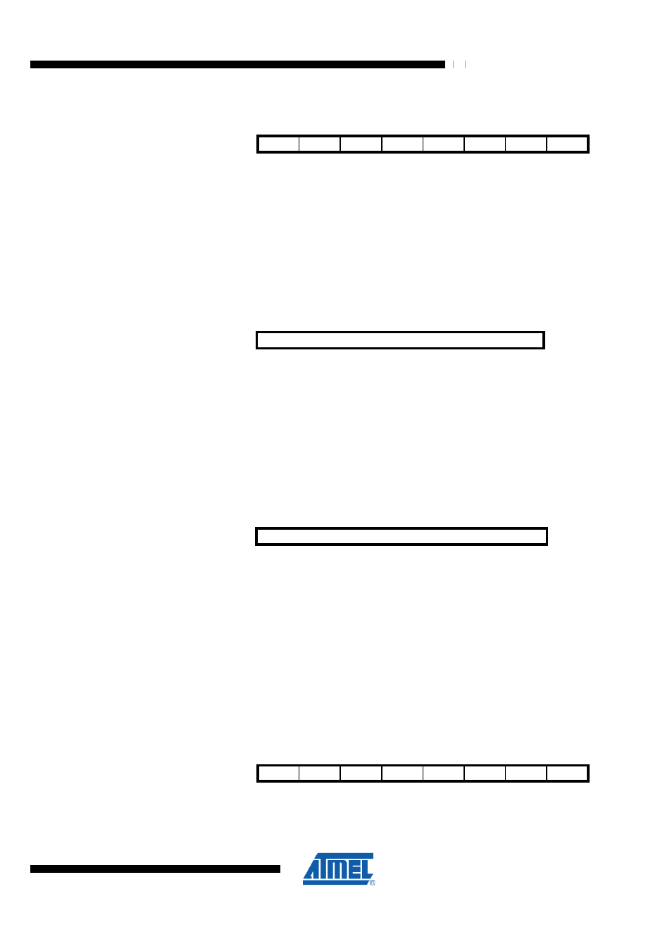
14.4.8 DDRD – Port D Data Direction Register
Bit
7
6
5
4
3
2
1
0
$0A ($2A)
DDD7
DDD6
DDD5
DDD4
DDD3
DDD2
DDD1
DDD0
DDRD
Read/Write
RW
RW
RW
RW
RW
RW
RW
RW
Initial Value
0
0
0
0
0
0
0
0
The DDDn bit in the DDRD Register selects the direction of the PORTD pin n. If DDDn
is written logic one, PDn is configured as an output pin. If DDDn is written logic zero,
PDn is configured as an input pin.
•
Bit 7:0 – DDD7:0 - Port D Data Direction Register Value
14.4.9 PIND – Port D Input Pins Address
Bit
7
6
5
4
3
2
1
0
$09 ($29)
PIND7:0
PIND
Read/Write
R
R
R
R
R
R
R
R
Initial Value
0
0
0
0
0
0
0
0
This register allows access to the PORTD pins independent of the setting of the Data
Direction bit DDDn. The port pin can be read through the PINDn Register bit, and
writing a logic one to PINDn toggles the value of PORTDn.
•
Bit 7:0 – PIND7:0 - Port D Input Pins Value
14.4.10 PORTE – Port E Data Register
Bit
7
6
5
4
3
2
1
0
$0E ($2E)
PORTE7:0
PORTE
Read/Write
RW
RW
RW
RW
RW
RW
RW
RW
Initial Value
0
0
0
0
0
0
0
0
If PORTEn is written logic one when the PORTE pin n is configured as an input pin, the
pull-up resistor is activated. To switch the pull-up resistor off, PORTEn has to be written
logic zero or the pin has to be configured as an output pin. If PORTEn is written logic
one when the pin is configured as an output pin, the port pin is driven high (one). If
PORTEn is written logic zero when the pin is configured as an output pin, the port pin is
driven low (zero).
•
Bit 7:0 – PORTE7:0 - Port E Data Register Value
14.4.11 DDRE – Port E Data Direction Register
Bit
7
6
5
4
3
2
1
0
$0D ($2D)
DDE7
DDE6
DDE5
DDE4
DDE3
DDE2
DDE1
DDE0
DDRE
Read/Write
RW
RW
RW
RW
RW
RW
RW
RW
Initial Value
0
0
0
0
0
0
0
0