4 phase correct pwm mode – Rainbow Electronics ATmega128RFA1 User Manual
Page 235
235
8266A-MCU Wireless-12/09
ATmega128RFA1
equal to MAX will result in a constantly high or low output (depending on the polarity of
the output set by the COM0A1:0 bits.)
A frequency with 50% duty cycle waveform output in fast PWM mode can be achieved
by setting OC0x to toggle its logical level on each Compare Match (COM0x1:0 = 1). The
generated waveform will have a maximum frequency of f
OC0xPWM
= f
clk_I/O
/2 when
OCR0A is set to zero. This feature is similar to the OC0A toggle in CTC mode, except
that in the fast PWM mode the double buffer feature of the Output Compare unit is
enabled.
17.7.4 Phase Correct PWM Mode
The phase correct pulse-width modulation (PWM) mode (WGM02:0 = 1 or 5) provides a
phase-correct, high-resolution PWM waveform generation option. The phase correct
PWM mode is based on a dual-slope operation. The counter counts repeatedly from
BOTTOM to TOP and then from TOP to BOTTOM. TOP is defined as 0xFF when
WGM2:0 = 1 and TOP = OCR0A when WGM2:0 = 5. In non-inverting Compare Output
mode, the Output Compare (OC0x) is cleared on the Compare Match between TCNT0
and OCR0x while up-counting, and OC0x is set on the Compare Match while down-
counting. The operation is inverted in inverting Output Compare mode. The dual-slope
operation has a lower maximum operation frequency than single-slope operation.
However, due to the symmetric feature of the dual-slope PWM modes, these modes are
preferred for motor control applications.
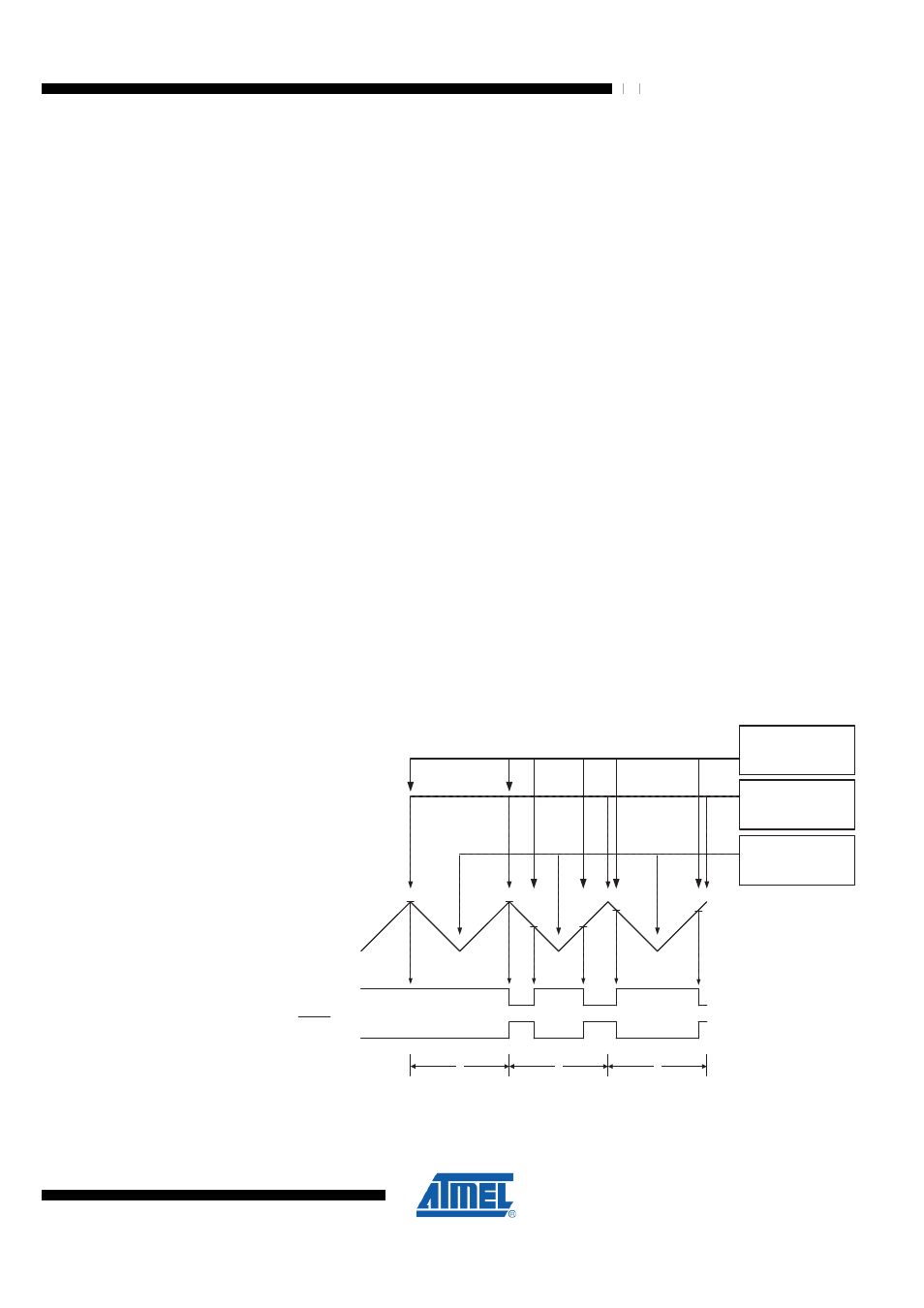
In phase correct PWM mode the counter is incremented until the counter value matches
TOP. The counter changes the direction when reaching TOP. The TCNT0 value will be
equal to TOP for one timer clock cycle. The timing diagram for the phase correct PWM
mode is shown in
. The TCNT0 value is shown in the timing diagram
as a histogram illustrating the dual-slope operation. The diagram includes non-inverted
and inverted PWM outputs. The small horizontal line marks on the TCNT0 slopes
represent Compare Matches between OCR0x and TCNT0.
Figure 17-7. Phase Correct PWM Mode Timing Diagram
TOVn Interrupt Flag Set
OCnx Interrupt Flag Set
1
2
3
TCNTn
Period
OCnx
OCnx
(COMnx1:0 = 2)
(COMnx1:0 = 3)
OCRnx Update
The Timer/Counter Overflow Flag (TOV0) is set each time the counter reaches
BOTTOM. The Interrupt Flag can be used to generate an interrupt each time the
counter reaches the BOTTOM value.