6 didr0 - digital input disable register 0, 7 didr2 - digital input disable register 2, 8 bgcr - reference voltage calibration register – Rainbow Electronics ATmega128RFA1 User Manual
Page 433: Atmega128rfa1
433
8266A-MCU Wireless-12/09
ATmega128RFA1
•
ADC9:0: A/D Conversion Result
These bits represent the result from the conversion as detailed in
.
27.11.6 DIDR0 – Digital Input Disable Register 0
Bit
7
6
5
4
3
2
1
0
NA ($7E)
ADC7D
ADC6D
ADC5D
ADC4D
ADC3D
ADC2D
ADC1D
ADC0D
DIDR0
Read/Write
RW
RW
RW
RW
RW
RW
RW
RW
Initial Value
0
0
0
0
0
0
0
0
•
Bits 7:0 – ADC7D:ADC0D: Digital Input Disable
When this bit is written logic one, the digital input buffer on the corresponding ADC pin
is disabled. The corresponding PIN Register bit will always read as zero when this bit is
set. When an analog signal is applied to the ADC7:0 pin and the digital input from this
pin is not needed, this bit should be written logic one to reduce power consumption in
the digital input buffer.
27.11.7 DIDR2 – Digital Input Disable Register 2
Bit
7
6
5
4
3
2
1
0
NA ($7D)
ADC15D ADC14D ADC13D ADC12D ADC11D ADC10D ADC9D
ADC8D
DIDR2
Read/Write
RW
RW
RW
RW
RW
RW
RW
RW
Initial Value
0
0
0
0
0
0
0
0
Reserved for future use.
•
Bit 7:0 – ADC15D:ADC8D - Reserved Bits
This bit is reserved for future use. For ensuring compatibility with future devices, this bit
must be written to zero.
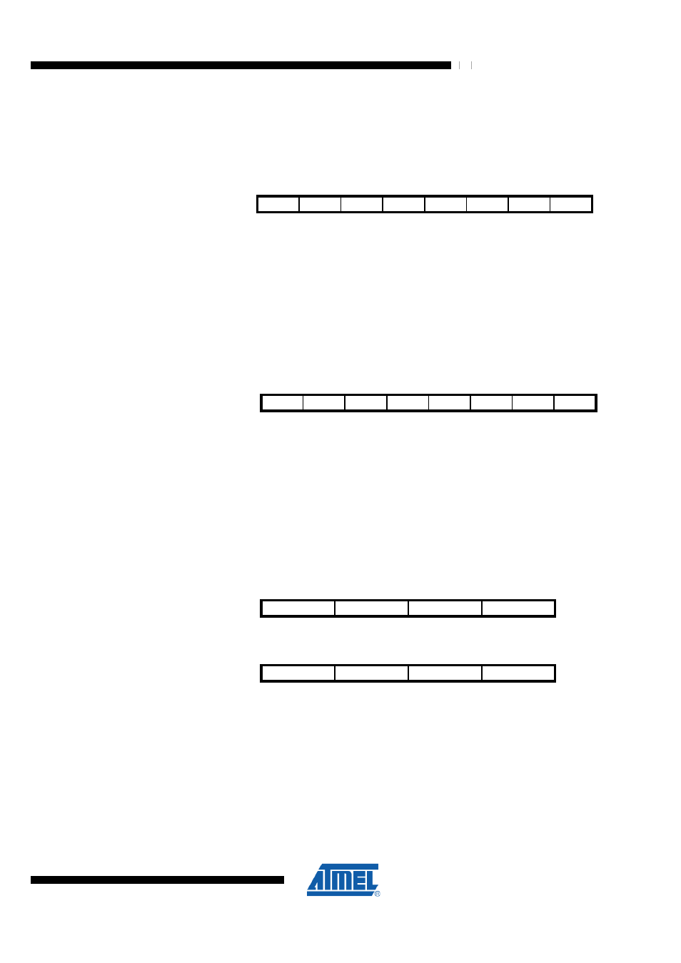
27.11.8 BGCR – Reference Voltage Calibration Register
Bit
7
6
5
4
NA ($67)
Res
BGCAL_FINE3
BGCAL_FINE2
BGCAL_FINE1
BGCR
Read/Write
R
RW
RW
RW
Initial Value
0
0
0
0
Bit
3
2
1
0
NA ($67)
BGCAL_FINE0
BGCAL2
BGCAL1
BGCAL0
BGCR
Read/Write
RW
RW
RW
RW
Initial Value
0
0
0
0
This register contains the calibration values of the reference voltage of the ADC. The
values are loaded from the fuse memory after power-up. They can be corrected by the
application software e.g. to compensate for temperature changes. The internal 1.6V
reference voltage is calibrated and has therefore the highest accuracy compared to the
1.5V or AVDD reference.
•
Bit 7 – Res - Reserved Bit
This bit is reserved for future use. A read access always will return zero. A write access
does not modify the content.