2 adcsrb - adc control and status register b, Atmega128rfa1 – Rainbow Electronics ATmega128RFA1 User Manual
Page 428
428
8266A-MCU Wireless-12/09
ATmega128RFA1
ADCSRA is set). Note that the MUX5 bit is located in the ADCSRB register. A write
access to the MUX4:0 bits triggers the update of the internally buffered MUX5 bit, see
"Accessing the ADMUX Register" on page 417
.
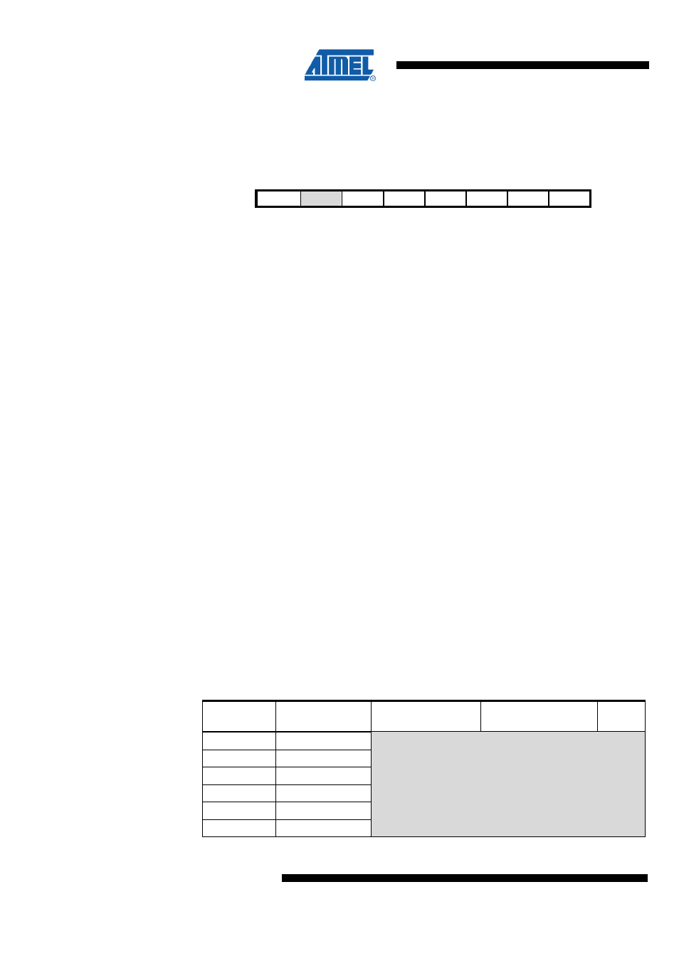
27.11.2 ADCSRB – ADC Control and Status Register B
Bit
7
6
5
4
3
2
1
0
NA ($7B)
AVDDOK
ACME
REFOK
ACCH
MUX5
ADTS2
ADTS1
ADTS0
ADCSRB
Read/Write
R
R/W
R
R/W
R/W
R/W
R/W
R/W
Initial Value
0
0
0
0
0
0
0
0
•
Bit 7 – AVDDOK: AVDD Supply Voltage OK
The analog functions of the ADC are powered from the AVDD domain. AVDD is
supplied from an internal voltage regulator. Setting the ADEN bit in register ADCSRA
will power-up the AVDD domain if not already requested by another functional group of
the device. The bit allows the user to monitor (poll) the status of the AVDD domain. A
status of 1 indicates that AVDD has been powered-up.
•
Bit 6 – ACME: Analog Comparator Multiplexer Enable
This bit is used for the Analog Comparator only. See
Status Register B" on page 409
for details.
•
Bit 5 – REFOK: Reference Voltage OK
The status of the internal generated reference voltage can be monitored through this
bit. Setting the ADEN bit in register ADCSRA will enable the reference voltage for the
ADC according to the REFSn bits in the ADMUX register. The reference voltage will be
available after a start-up delay. A REFOK value of 1 indicates that the internal
generated reference voltage is approaching final levels.
•
Bit 4 – ACCH: Analog Channel Change
The user can force a reset of the analog blocks by setting this bit to 1 without
requesting a different channel. The analog blocks of the ADC will be reset to handle
possible new voltage ranges. Such a reset phase is especially important for the gain
amplifier. It could be temporarily disabled by a large step of its input common voltage
leading to erroneous A/D conversion results. ACCH will read as one until the reset
phase of the analog blocks can be entered.
•
Bit 3 – MUX5: Analog Channel and Gain Selection Bit
This bit is used together with MUX4:0 in ADMUX to select the analog input signals
connected to the ADC. See the following table for details. If this bit is changed during a
conversion, the change will not go in effect until this conversion is complete. Note that
the MUX5 bit is internally buffered and a write access to the MUX4:0 bits is required to
trigger the update of the MUX5 bit, see
"Accessing the ADMUX Register" on page 417
.
Table 27-11. Input Channel Selections
MUX5:0
Single Ended
Input
Positive Differential
Input
Negative Differential
Input
Gain
000000
ADC0
000001
ADC1
000010
ADC2
000011
ADC3
000100
ADC4
000101
ADC5
N/A