Atmega128rfa1 – Rainbow Electronics ATmega128RFA1 User Manual
Page 239
239
8266A-MCU Wireless-12/09
ATmega128RFA1
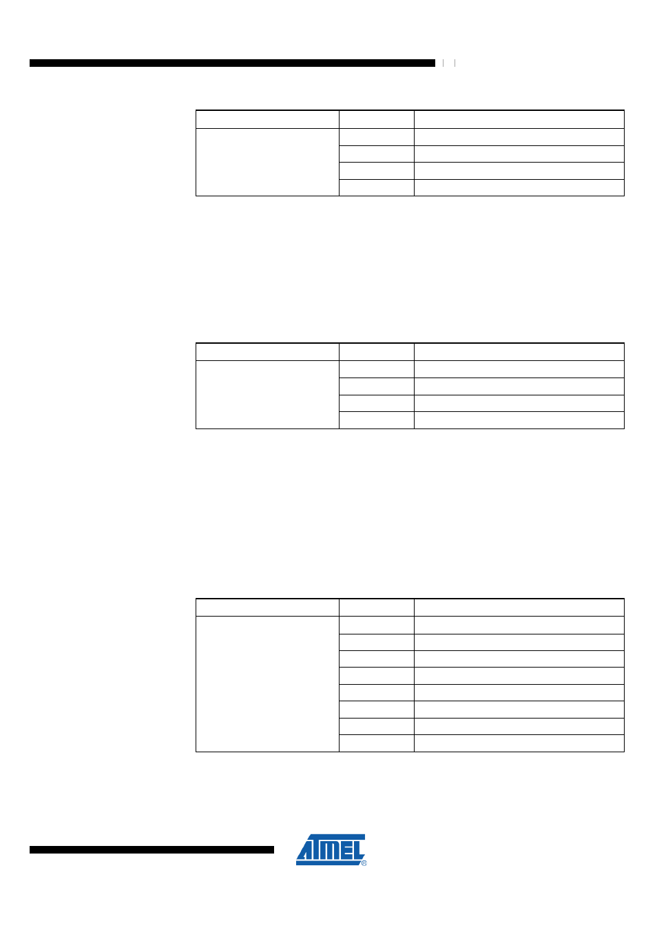
Table 17-6 COM0A Register Bits
Register Bits
Value
Description
0
Normal port operation, OC0A disconnected
1
Toggle OC0A on Compare Match
2
Clear OC0A on Compare Match
COM0A1:0
3
Set OC0A on Compare Match
•
Bit 5:4 – COM0B1:0 - Compare Match Output B Mode
These bits control the Output Compare pin (OC0B) behavior. If one or both of the
COM0B1:0 bits are set, the OC0B output overrides the normal port functionality of the
I/O pin it is connected to. However, note that the Data Direction Register (DDR) bit
corresponding to the OC0B pin must be set in order to enable the output driver. When
OC0B is connected to the pin, the function of the COM0B1:0 bits depends on the
WGM02:0 bit setting. The following shows the COM0B1:0 bit functionality when the
WGM02:0 bits are set to a normal or CTC mode (non-PWM). For the functionality in
other modes refer to section "Operating Modes".
Table 17-7 COM0B Register Bits
Register Bits
Value
Description
0
Normal port operation, OC0B disconnected
1
Toggle OC0B on Compare Match
2
Clear OC0B on Compare Match
COM0B1:0
3
Set OC0B on Compare Match
•
Bit 3:2 – Res1:0 - Reserved Bit
This bit is reserved for future use. A read access always will return zero. A write access
does not modify the content.
•
Bit 1:0 – WGM01:00 - Waveform Generation Mode
Combined with the WGM02 bit found in the TCCR0B Register, these bits control the
counting sequence of the counter, the source for maximum (TOP) counter value, and
what type of waveform generation to be used according to the following table. Modes of
operation supported by the Timer/Counter0 unit are: Normal mode (counter), Clear
Timer on Compare Match (CTC) mode, and two types of Pulse Width Modulation
(PWM) modes (see section "Modes of Operation" for details).
Table 17-8 WGM0 Register Bits
Register Bits
Value
Description
0x0
Normal mode of operation
0x1
PWM, phase correct, TOP=0xFF
0x2
CTC, TOP = OCRA
0x3
Fast PWM, TOP=0xFF
0x4
Reserved
0x5
PWM, Phase correct, TOP = OCRA
0x6
Reserved
WGM01:00
0x7
Fast PWM, TOP=OCRA