Atmega128rfa1 – Rainbow Electronics ATmega128RFA1 User Manual
Page 359
359
8266A-MCU Wireless-12/09
ATmega128RFA1
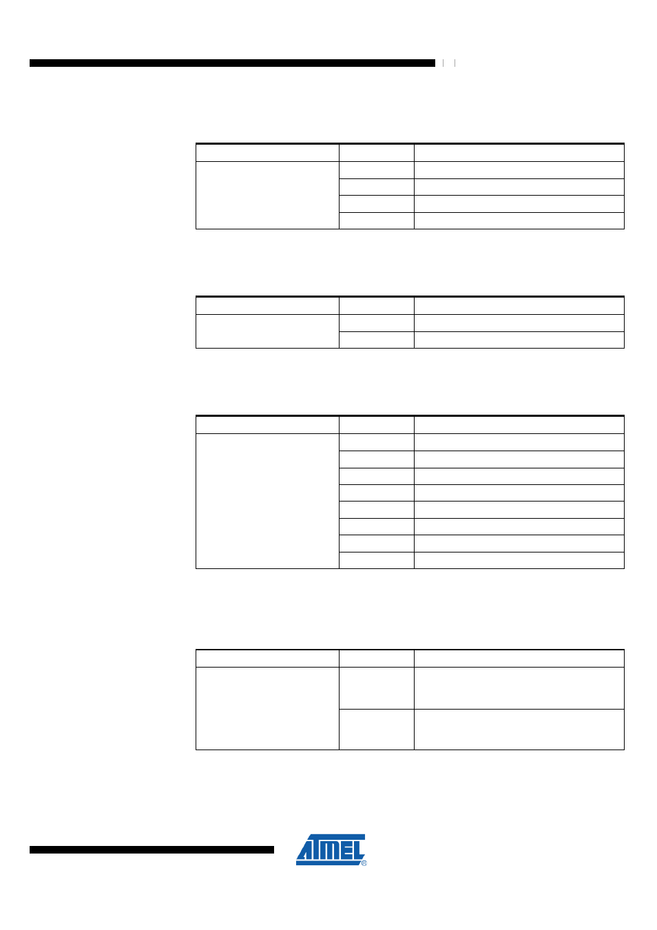
compare it to the UPM0 setting. If a mismatch is detected, the UPE0 Flag in UCSR0A
will be set.
Table 23-5 UPM0 Register Bits
Register Bits
Value
Description
0x00
Disabled
0x01
Reserved
0x02
Enabled, Even Parity
UPM01:00
0x03
Enabled, Odd Parity
•
Bit 3 – USBS0 - Stop Bit Select
This bit selects the number of stop bits to be inserted by the Transmitter. The Receiver
ignores this setting.
Table 23-6 USBS0 Register Bits
Register Bits
Value
Description
0x00
1-bit
USBS0
0x01
2-bit
•
Bit 2:1 – UCSZ01:00 - Character Size
The UCSZ01:0 bits combined with the UCSZ02 bit in UCSR0B sets the number of data
bits (Character Size) in the frame that the Receiver and Transmitter use.
Table 23-7 UCSZ0 Register Bits
Register Bits
Value
Description
0
5-bit
1
6-bit
2
7-bit
3
8-bit
4
Reserved
5
Reserved
6
Reserved
UCSZ01:00
7
9-bit
•
Bit 0 – UCPOL0 - Clock Polarity
This bit is used for synchronous mode only. Write this bit to zero when asynchronous
mode is used. The UCPOL0 bit sets the relationship between data output change and
data input sample, and the synchronous clock (XCK0).
Table 23-8 UCPOL0 Register Bits
Register Bits
Value
Description
0
Rising XCKn Edge (Transmitted Data
Changed), Falling XCKn Edge (Received
Data Sampled)
UCPOL0
1
Falling XCKn Edge (Transmitted Data
Changed), Rising XCKn Edge (Received
Data Sampled)