10 register description, 1 udr0 - usart0 i/o data register, 2 ucsr0a - usart0 control and status register a – Rainbow Electronics ATmega128RFA1 User Manual
Page 356: Atmega128rfa1
356
8266A-MCU Wireless-12/09
ATmega128RFA1
Do not use read-modify-write instructions (SBI and CBI) to set or clear the MPCMn bit.
The MPCMn bit shares the same I/O location as the TXCn flag and this might
accidentally be cleared when using SBI or CBI instructions.
23.10 Register Description
23.10.1 UDR0 – USART0 I/O Data Register
Bit
7
6
5
4
3
2
1
0
NA ($C6)
UDR07:00
UDR0
Read/Write
RW
RW
RW
RW
RW
RW
RW
RW
Initial Value
0
0
0
0
0
0
0
0
The USART Transmit Data Buffer Register and USART Receive Data Buffer Registers
share the same I/O address referred to as USART Data Register or UDR0. The
Transmit Data Buffer Register (TXB) will be the destination for data written to the UDR0
Register location. Reading the UDR0 Register location will return the contents of the
Receive Data Buffer Register (RXB). For 5-, 6-, or 7-bit characters the upper unused
bits will be ignored by the Transmitter and set to zero by the Receiver. The transmit
buffer can only be written when the UDRE0 Flag in the UCSR0A Register is set. Data
written to UDR0 when the UDRE0 Flag is not set, will be ignored by the USART
Transmitter. When data is written to the transmit buffer and the Transmitter is enabled,
the Transmitter will load the data into the Transmit Shift Register when the Shift
Register is empty. Then the data will be serially transmitted on the TxD0 pin. The
receive buffer consists of a two level FIFO. The FIFO will change its state whenever the
receive buffer is accessed. Due to this behavior of the receive buffer, do not use Read-
Modify-Write instructions (SBI and CBI) on this location. Be careful when using bit test
instructions (SBIC and SBIS), since these also will change the state of the FIFO.
•
Bit 7:0 – UDR07:00 - USART I/O Data Register
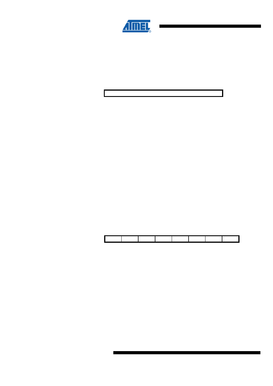
23.10.2 UCSR0A – USART0 Control and Status Register A
Bit
7
6
5
4
3
2
1
0
NA ($C0)
RXC0
TXC0
UDRE0
FE0
DOR0
UPE0
U2X0
MPCM0
UCSR0A
Read/Write
R
RW
R
R
R
R
RW
RW
Initial Value
0
0
1
0
0
0
0
0
•
Bit 7 – RXC0 - USART Receive Complete
This flag bit is set when there are unread data in the receive buffer and cleared when
the receive buffer is empty (i.e., does not contain any unread data). If the Receiver is
disabled, the receive buffer will be flushed and consequently the RXC0 bit will become
zero. The RXC0 Flag can be used to generate a Receive Complete interrupt (see
description of the RXCIE0 bit).
•
Bit 6 – TXC0 - USART Transmit Complete
This flag bit is set when the entire frame in the Transmit Shift Register has been shifted
out and there are no new data currently present in the transmit buffer (UDR0). The
TXC0 Flag bit is automatically cleared when a transmit complete interrupt is executed,
or it can be cleared by writing a one to its bit location. The TXC0 Flag can generate a
Transmit Complete interrupt (see description of the TXCIE0 bit).