Atmega128rfa1 – Rainbow Electronics ATmega128RFA1 User Manual
Page 253
253
8266A-MCU Wireless-12/09
ATmega128RFA1
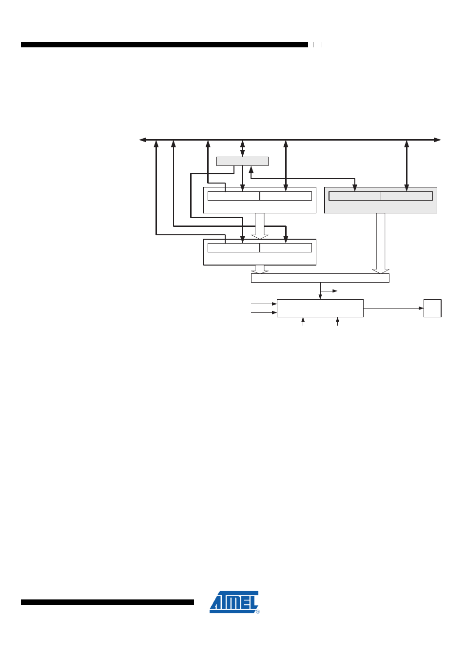
Figure 18-4 shows a block diagram of the Output Compare unit. The small “n” in the
register and bit names indicates the device number (n = Timer/Counter n), and the “x”
indicates Output Compare unit A, B or C. The elements of the block diagram not direct
parts of the Output Compare unit are gray shaded.
Figure 18-4. Output Compare Unit Block Diagram
OCFnx (Int.Req.)
=
(16-bit Comparator )
OCRnx Buffer (16-bit Register)
OCRnxH Buf. (8-bit)
OCnx
TEMP (8-bit)
DATA BUS
(8-bit)
OCRnxL Buf. (8-bit)
TCNTn (16-bit Counter)
TCNTnH (8-bit)
TCNTnL (8-bit)
COMnx1:0
WGMn3:0
OCRnx (16-bit Register)
OCRnxH (8-bit)
OCRnxL (8-bit)
Waveform Generator
TOP
BOTTOM
The OCRnx Register is double buffered when using any of the twelve Pulse Width
Modulation (PWM) modes. For the Normal and Clear Timer on Compare (CTC) modes
of operation, the double buffering is disabled. The double buffering synchronizes the
update of the OCRnx Compare Register to either TOP or BOTTOM of the counting
sequence. The synchronization prevents the occurrence of odd-length, non-symmetrical
PWM pulses, thereby making the output glitch-free.
The OCRnx Register access may seem complex, but this is not the case. When the
double buffering is enabled, the CPU has access to the OCRnx Buffer Register. If
double buffering is disabled the CPU will access the OCRnx directly. The content of the
OCR1x (Buffer or Compare) Register is only changed by a write operation (the
Timer/Counter does not update this register automatically as the TCNT1 and ICR1
Register). Therefore OCR1x is not read via the high byte temporary register (TEMP).
However, it is a good practice to read the low byte first similar to accessing other 16-bit
registers. Writing the OCRnx Registers must be done via the TEMP Register since the
compare of all 16 bits is done continuously. The high byte (OCRnxH) has to be written
first. The TEMP Register will be updated with the value written by the CPU to the high
byte I/O location. Then when the low byte (OCRnxL) is written to the lower eight bits,
the high byte will be copied into the upper 8-bits of either the OCRnx buffer or OCRnx
Compare Register in the same system clock cycle.
For more information of how to access the 16-bit registers refer to
.