16 tccr3a - timer/counter3 control register a, Atmega128rfa1 – Rainbow Electronics ATmega128RFA1 User Manual
Page 276
276
8266A-MCU Wireless-12/09
ATmega128RFA1
overflows. TOV1 is automatically cleared when the Timer/Counter1 Overflow Interrupt
Vector is executed. Alternatively, TOV1 can be cleared by writing a logic one to its bit
location.
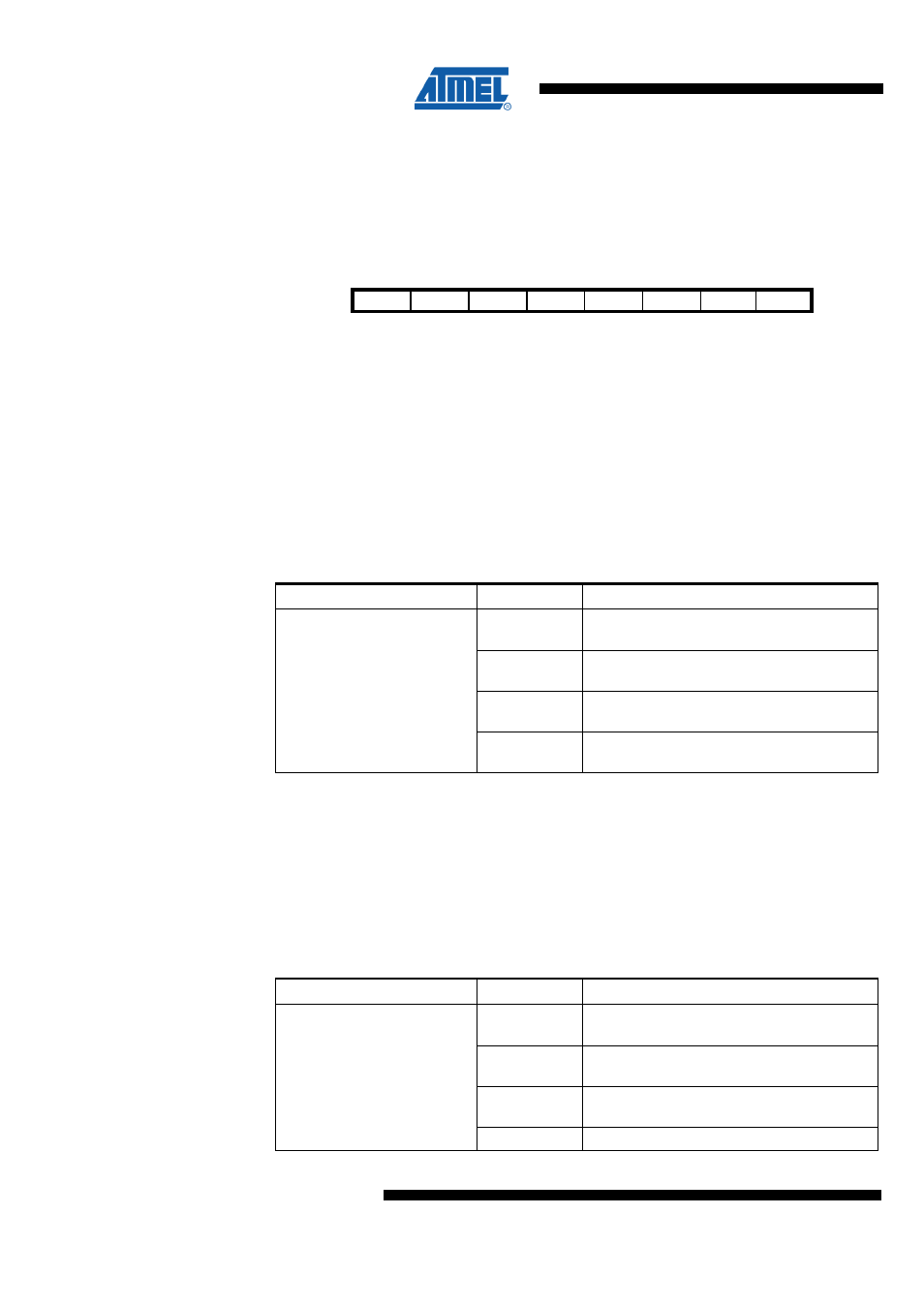
18.11.16 TCCR3A – Timer/Counter3 Control Register A
Bit
7
6
5
4
3
2
1
0
NA ($90)
COM3A1 COM3A0 COM3B1 COM3B0 COM3C1 COM3C0 WGM31 WGM30
TCCR3A
Read/Write
RW
RW
RW
RW
RW
RW
RW
RW
Initial Value
0
0
0
0
0
0
0
0
•
Bit 7:6 – COM3A1:0 - Compare Output Mode for Channel A
The COM3A1:0 bits control the output compare behavior of pin OC3A. If one or both of
the COM3A1:0 bits are written to one, the OC3A output overrides the normal port
functionality of the I/O pin it is connected to. However note that the Data Direction
Register (DDR) bit corresponding to the OC3A pin must be set in order to enable the
output driver. When the OC3A is connected to the pin, the function of the COM3A1:0
bits is dependent of the WGM33:0 bits setting. The following table shows the
COM3A1:0 bit functionality when the WGM33:0 bits are set to a normal or a CTC mode
(non-PWM). For the other functionality refer to section "Modes of Operation".
Table 18-12 COM3A Register Bits
Register Bits
Value
Description
0
Normal port operation, OCnA/OCnB/OCnC
disconnected.
1
Toggle OCnA/OCnB/OCnC on Compare
Match.
2
Clear OCnA/OCnB/OCnC on Compare
Match (set output to low level).
COM3A1:0
3
Set OCnA/OCnB/OCnC on Compare Match
(set output to high level).
•
Bit 5:4 – COM3B1:0 - Compare Output Mode for Channel B
The COM3B1:0 bits control the output compare behavior of pin OC3B. If one or both of
the COM3B1:0 bits are written to one, the OC3B output overrides the normal port
functionality of the I/O pin it is connected to. However note that the Data Direction
Register (DDR) bit corresponding to the OC3B pin must be set in order to enable the
output driver. When the OC3B is connected to the pin, the function of the COM3B1:0
bits is dependent of the WGM33:0 bits setting. The following table shows the
COM3B1:0 bit functionality when the WGM33:0 bits are set to a normal or a CTC mode
(non-PWM). For the other functionality refer to section "Modes of Operation".
Table 18-13 COM3B Register Bits
Register Bits
Value
Description
0
Normal port operation, OCnA/OCnB/OCnC
disconnected.
1
Toggle OCnA/OCnB/OCnC on Compare
Match.
2
Clear OCnA/OCnB/OCnC on Compare
Match (set output to low level).
COM3B1:0
3
Set OCnA/OCnB/OCnC on Compare Match