Atmega128rfa1 – Rainbow Electronics ATmega128RFA1 User Manual
Page 269
269
8266A-MCU Wireless-12/09
ATmega128RFA1
Combined with the WGM11:0 bits found in the TCCR1A Register, these bits control the
counting sequence of the counter, the source for maximum (TOP) counter value, and
what type of waveform generation to be used. Modes of operation supported by the
Timer/Counter unit are: Normal mode (counter), Clear Timer on Compare match (CTC)
mode, and three types of Pulse Width Modulation (PWM) modes. For more information
on the different modes see section "Modes of Operation".
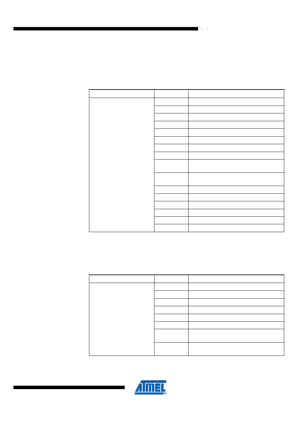
Table 18-10 WGM1 Register Bits
Register Bits
Value
Description
0x0
Normal mode of operation
0x1
PWM, phase correct, 8-bit
0x2
PWM, phase correct, 9-bit
0x3
PWM, phase correct, 10-bit
0x4
CTC, TOP = OCRnA
0x5
Fast PWM, 8-bit
0x6
Fast PWM, 9-bit
0x7
Fast PWM, 10-bit
0x8
PWM, Phase and frequency correct, TOP =
ICRn
0x9
PWM, Phase and frequency correct, TOP =
OCRnA
0xA
PWM, Phase correct, TOP = ICRn
0xB
PWM, Phase correct, TOP = OCRnA
0xC
CTC, TOP = OCRnA
0xD
Reserved
0xE
Fast PWM, TOP = ICRn
WGM11:10
0xF
Fast PWM, TOP = OCRnA
•
Bit 2:0 – CS12:10 - Clock Select
The three clock select bits select the clock source to be used by the Timer/Counter1
according to the following table. If external pin modes are used for the Timer/Counter1,
transitions on the T1 pin will clock the counter even if the pin is configured as an output.
This feature allows software control of the counting.
Table 18-11 CS1 Register Bits
Register Bits
Value
Description
0x00
No clock source (Timer/Counter stopped)
0x01
clk_IO/1 (no prescaling)
0x02
clk_IO/8 (from prescaler)
0x03
clk_IO/64 (from prescaler)
0x04
clk_IO/256 (from prescaler)
0x05
clk_IO/1024 (from prescaler)
0x06
External clock source on Tn pin, clock on
falling edge
CS12:10
0x07
External clock source on Tn pin, clock on
rising edge