15 pinf - port f input pins address, 16 portg - port g data register, 17 ddrg - port g data direction register – Rainbow Electronics ATmega128RFA1 User Manual
Page 209: Atmega128rfa1

209
8266A-MCU Wireless-12/09
ATmega128RFA1
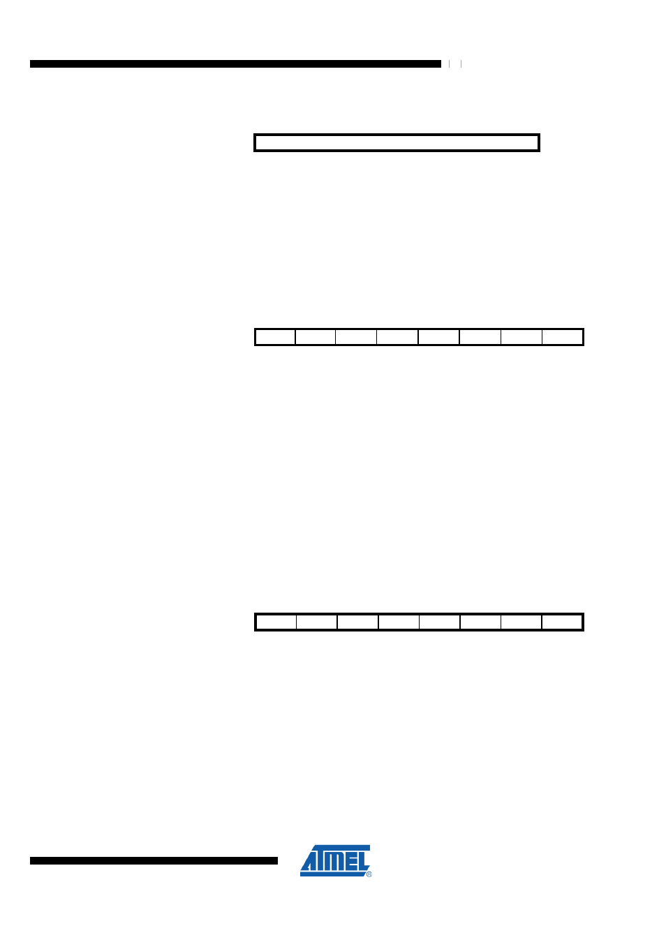
14.4.15 PINF – Port F Input Pins Address
Bit
7
6
5
4
3
2
1
0
$0F ($2F)
PINF7:0
PINF
Read/Write
R
R
R
R
R
R
R
R
Initial Value
0
0
0
0
0
0
0
0
This register allows access to the PORTF pins independent of the setting of the Data
Direction bit DDFn. The port pin can be read through the PINFn Register bit, and writing
a logic one to PINFn toggles the value of PORTFn.
•
Bit 7:0 – PINF7:0 - Port F Input Pins Value
14.4.16 PORTG – Port G Data Register
Bit
7
6
5
4
3
2
1
0
$14 ($34)
Res1
Res0
PORTG5 PORTG4 PORTG3 PORTG2 PORTG1 PORTG0
PORTG
Read/Write
R
R
RW
RW
RW
RW
RW
RW
Initial Value
0
0
0
0
0
0
0
0
If PORTGn is written logic one when the PORTG pin n is configured as an input pin, the
pull-up resistor is activated. To switch the pull-up resistor off, PORTGn has to be written
logic zero or the pin has to be configured as an output pin. If PORTGn is written logic
one when the pin is configured as an output pin, the port pin is driven high (one). If
PORTGn is written logic zero when the pin is configured as an output pin, the port pin is
driven low (zero).
•
Bit 7:6 – Res1:0 - Reserved Bit
This bit is reserved for future use. A read access always will return zero. A write access
does not modify the content.
•
Bit 5:0 – PORTG5:0 - Port G Data Register Value
14.4.17 DDRG – Port G Data Direction Register
Bit
7
6
5
4
3
2
1
0
$13 ($33)
Res1
Res0
DDG5
DDG4
DDG3
DDG2
DDG1
DDG0
DDRG
Read/Write
R
R
RW
RW
RW
RW
RW
RW
Initial Value
0
0
0
0
0
0
0
0
The DDGn bit in the DDRG Register selects the direction of the PORTG pin n. If DDGn
is written logic one, PGn is configured as an output pin. If DDGn is written logic zero,
PGn is configured as an input pin.
•
Bit 7:6 – Res1:0 - Reserved Bit
This bit is reserved for future use. A read access always will return zero. A write access
does not modify the content.
•
Bit 5:0 – DDG5:0 - Port G Data Direction Register Value
