Figure 31-1 on, Table 31-9 on, Atmega128rfa1 – Rainbow Electronics ATmega128RFA1 User Manual
Page 468
468
8266A-MCU Wireless-12/09
ATmega128RFA1
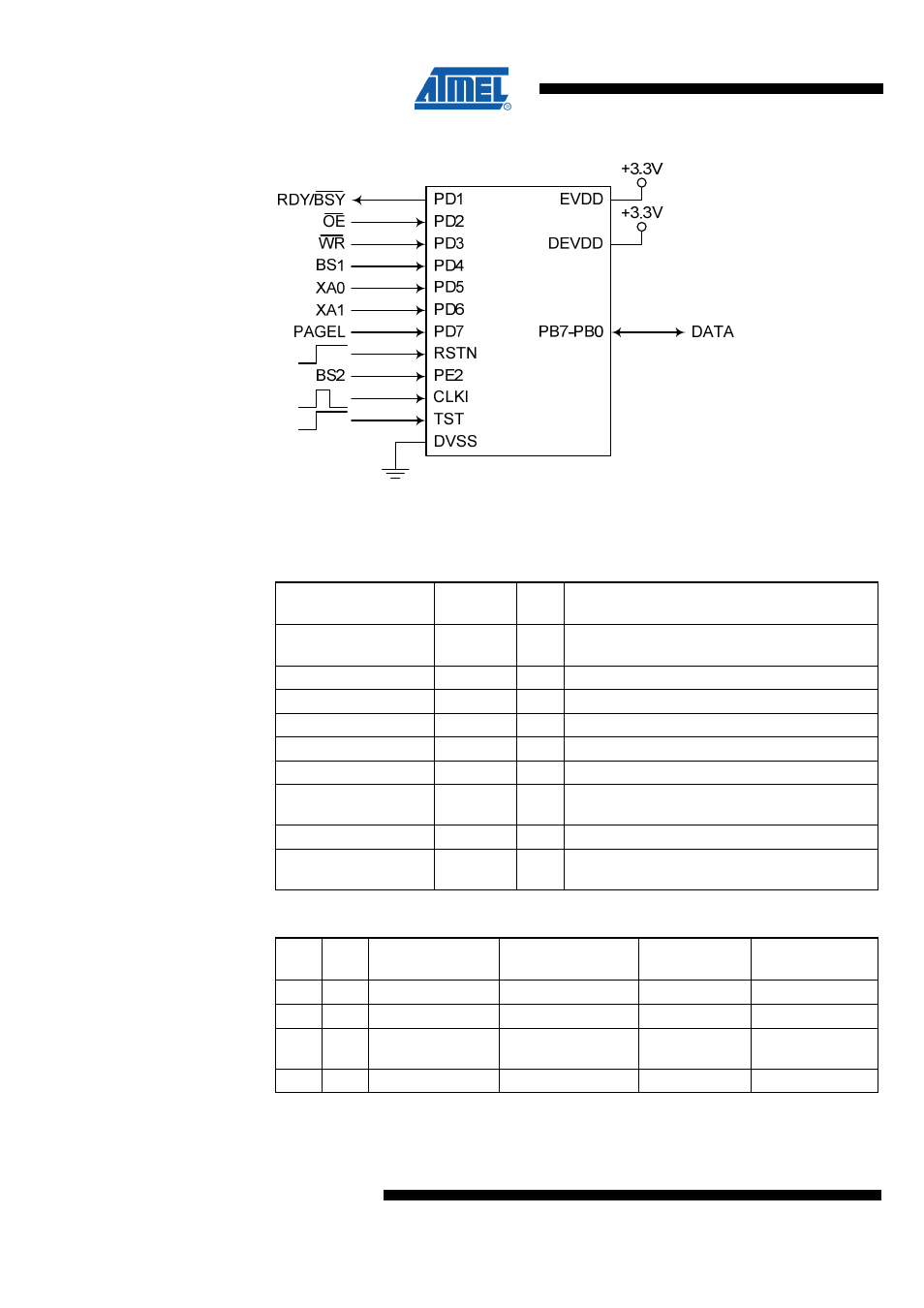
Figure 31-1. Parallel Programming
(1)
Note:
1. Unused Pins should be left floating.
Table 31-9. Pin Name Mapping
Signal Name in
Programming Mode
Pin Name
I/O
Function
RDY/BSY
___
PD1
O
0: Device is busy programming, 1: Device is
ready for new command.
OE
__
PD2
I
Output Enable (Active low).
WR
___
PD3
I
Write Pulse (Active low).
BS1
PD4
I
Byte Select 1.
XA0
PD5
I
XTAL Action Bit 0.
XA1
PD6
I
XTAL Action Bit 1.
PAGEL
PD7
I
Program Memory and EEPROM data Page
Load.
BS2
PE2
I
Byte Select 2.
DATA
PB7-0
I/O
Bi-directional Data bus (Output when OE
¯ ¯ ¯ is
low).
Table 31-10. BS2 and BS1 Encoding
BS2
BS1
Flash / EEPROM
Address
Flash Data
Loading / Reading
Fuse
Programming
Reading Fuse
and Lock Bits
0
0
Low Byte
Low Byte
Low Byte
Fuse Low Byte
0
1
High Byte
High Byte
High Byte
Lock Bits
1
0
Extended High
Byte
Reserved
Extended Byte
Extended Fuse
Byte
1
1
Reserved
Reserved
Reserved
Fuse High Byte