Atmega128rfa1 – Rainbow Electronics ATmega128RFA1 User Manual
Page 424
424
8266A-MCU Wireless-12/09
ATmega128RFA1
For single ended conversion, the result is
REF
IN
V
V
ADC
1024
⋅
=
where V
IN
is the voltage on the selected input pin and V
REF
the selected voltage
). 0x000
represents analog ground, and 0x3FF represents the selected reference voltage minus
one LSB.
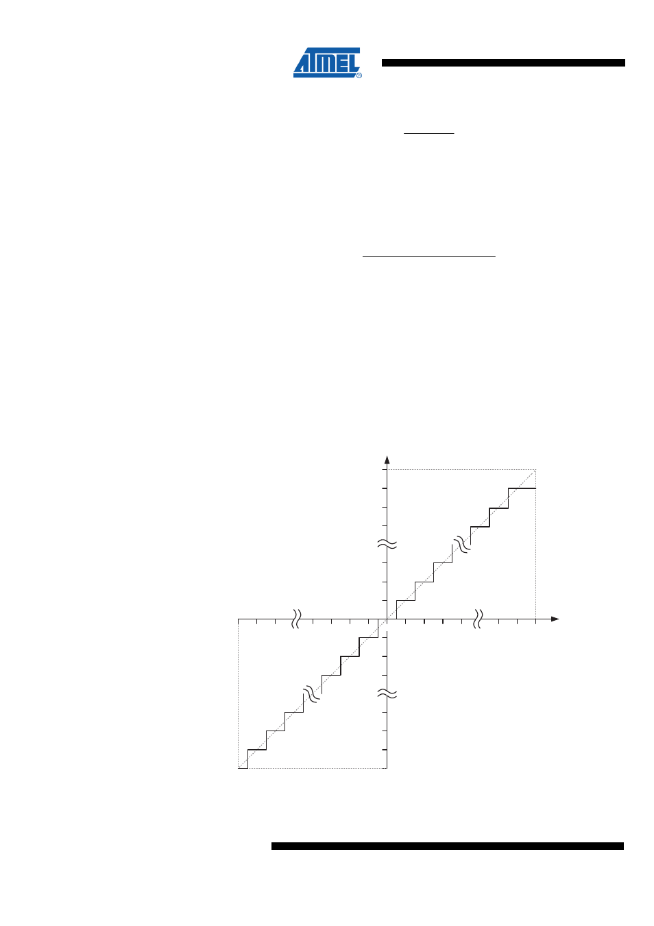
If differential channels are used, the result is
(
)
REF
NEG
POS
V
GAIN
V
V
ADC
512
⋅
⋅
−
=
where V
POS
is the voltage on the positive input pin, V
NEG
the voltage on the negative
input pin, and V
REF
the selected voltage reference. The result is presented in two’s
complement form, from 0x200 (-512d) through 0x1FF (+511d). Note that if the user
wants to perform a quick polarity check of the result, it is sufficient to read the MSB of
the result (ADC9 in ADCH). If the bit is one, the result is negative, and if this bit is zero,
the result is positive.
shows the decoding of the differential input
range.
page 425 shows the resulting output codes if the differential input
channel pair (ADCn - ADCm) is selected with a gain of GAIN and a reference voltage of
V
REF
.
Figure 27-16. Differential Measurement Range
0
Output code
0x1FF
0x000
V
REF
/GAIN
Differential Input
voltage (Volts)
0x3FF
0x200
- V
REF
/GAIN