1 compare output mode and waveform generation, Atmega128rfa1 – Rainbow Electronics ATmega128RFA1 User Manual
Page 255
255
8266A-MCU Wireless-12/09
ATmega128RFA1
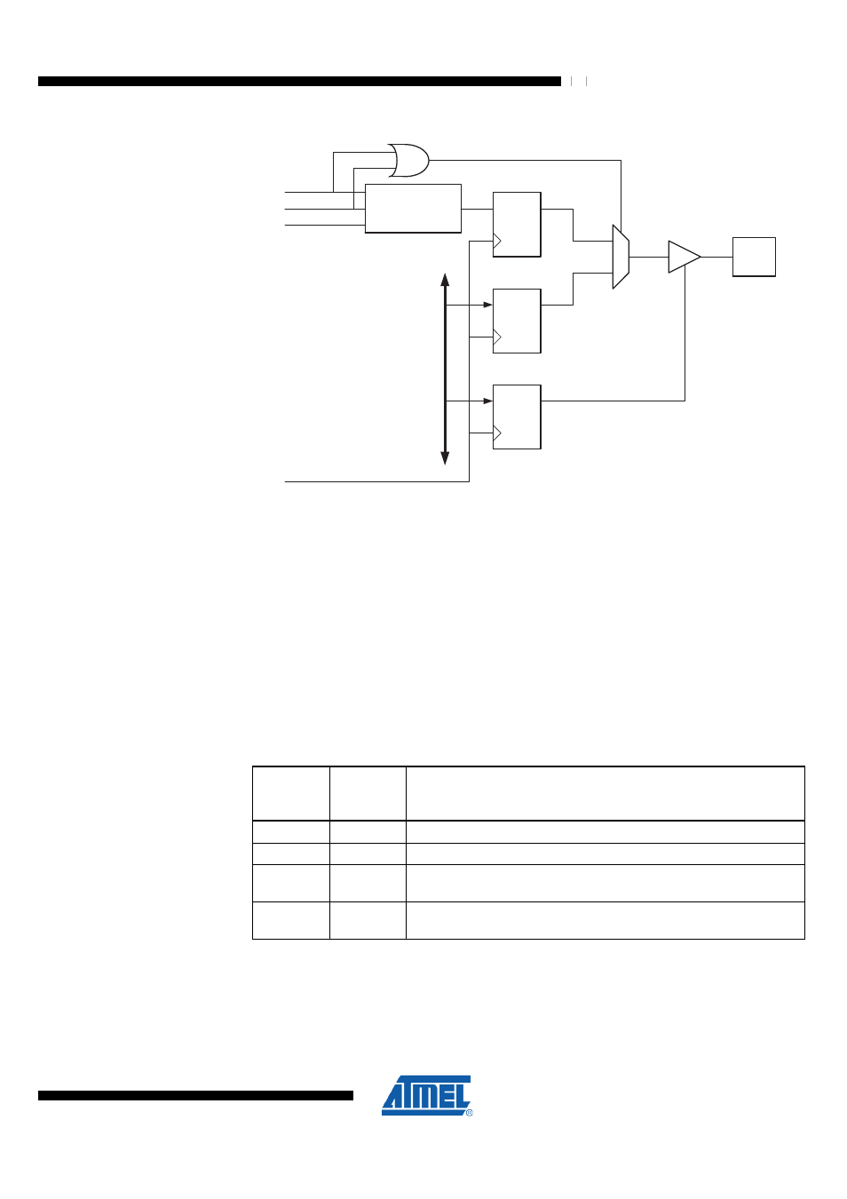
Figure 18-5. Compare Match Output Unit, Schematic
PORT
DDR
D
Q
D
Q
OCnx
Pin
OCnx
D
Q
Waveform
Generator
COMnx1
COMnx0
0
1
D
A
T
A B
US
FOCnx
clk
I/O
18.8.1 Compare Output Mode and Waveform Generation
The Waveform Generator uses the COMnx1:0 bits differently in normal, CTC and PWM
modes. A setting of COMnx1:0 = 0 tells the Waveform Generator in all modes that no
action on the OCnx Register is to be performed on the next compare match. For
compare output actions in the non-PWM modes refer to Table 18-2. For fast PWM
mode refer to Table 18-3 and for phase-correct and phase-and-frequency-correct PWM
refer to Table 18-4.
A change of the COMnx1:0 bits state will have effect at the first compare match after
the bits are written. For non-PWM modes, the action can be forced to have immediate
effect by using the FOCnx strobe bits.
Table 18-2 shows the COMnx1:0 bit functionality when the WGMn3:0 bits are set to a
normal or a CTC mode (non-PWM).
Table 18-2. Compare Output Mode, non-PWM
COMnA1
COMnB1
COMnC1
COMnA0
COMnB0
COMnC0
Description
0
0
Normal port operation, OCnA/OCnB/OCnC disconnected.
0
1
Toggle OCnA/OCnB/OCnC on compare match.
1
0
Clear OCnA/OCnB/OCnC on compare match (set output to low
level).
1
1
Set OCnA/OCnB/OCnC on compare match (set output to high
level).
Table 18-3 shows the COMnx1:0 bit functionality when the WGMn3:0 bits are set to the
fast PWM mode.