32 application circuits, 1 basic application schematic, Atmega128rfa1 – Rainbow Electronics ATmega128RFA1 User Manual
Page 493
493
8266A-MCU Wireless-12/09
ATmega128RFA1
32 Application Circuits
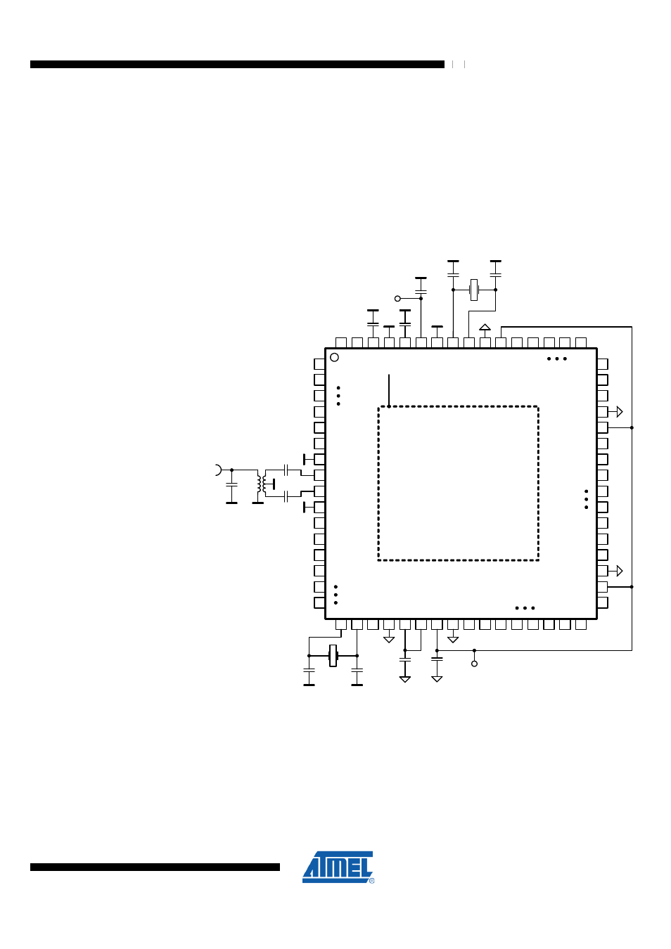
32.1 Basic Application Schematic
A basic application schematic of the ATmega128RFA1 with a single-ended RF
connector is shown in
. The 50Ω single-ended RF input is
transformed to the 100Ω differential RF port impedance using Balun B1. The capacitors
C1 and C2 provide AC coupling of the RF input to the RF port, capacitor C4 improves
matching.
Figure 32-1. Basic Application schematic (
Table 32-1 on page 494
)
8
7
6
5
4
3
2
1
17
18
19
20
21
22
23
24
56
57
58
59
60
61
62
63
ATmega128RFA1
A
R
E
F
A
V
S
S
AVSS
RFP
RFN
AVSS
TST
D
V
S
S
D
V
D
D
D
V
D
D
X
T
A
L
2
D
E
V
D
D
D
V
S
S
A
V
D
D
E
V
D
D
A
V
S
S
X
T
A
L
1
41
42
43
44
45
46
47
48
PB0
DVSS
PE0
PB7
CB3
CB4
RSTN
V
DD
XTAL
CX1
CX2
CB1
V
DD
CB2
C1
C2
B1
RF
C4
25
26
27
28
29
30
31
32
16
14
13
12
11
10
9
15
64
54
55
49
50
51
52
53
33
34
35
36
37
38
39
40
RSTON
CR1
XTAL
32kHz
CX3
CX4
CLKI
DEVDD
DVSS
DEVDD
P
E
7
D
V
S
S
D
E
V
D
D
P
F
0
PF7
PG0
P
G
5
P
D
0
P
D
7
The power supply bypass capacitors (CB2, CB4) are connected to the external analog
supply pin (EVDD, pin 59) and external digital supply pin (DEVDD, pin 23). Pins 34, 44
and 54 supply the digital port pins.
Capacitors CB1 and CB3 are bypass capacitors for the integrated analog and digital
voltage regulators to ensure stable operation and to improve noise immunity.
Capacitors should be placed as close as possible to the pins and should have a low-
resistance and low-inductance connection to ground to achieve the best performance.