5 state transition timing summary, Table 9-3 on, Atmega128rfa1 – Rainbow Electronics ATmega128RFA1 User Manual
Page 42
42
8266A-MCU Wireless-12/09
ATmega128RFA1
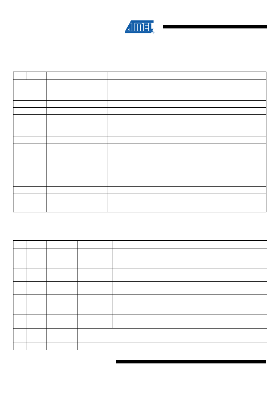
9.4.1.4.5 State Transition Timing Summary
The transition numbers correspond to
. See measurement setup in
"Basic Application Schematic" on page 493.
Table 9-3. Radio Transceiver State Transition Timing
No
Symbol
Transition
Time [µs], (typ)
Comments
1
t
TR2
SLEEP
TRX_OFF
240
Depends on crystal oscillator setup (CL = 10 pf)
TRX_OFF state indicated by TRX24_AWAKE interrupt
2
t
TR3
TRX_OFF
SLEEP
35 · 1 / f
CLKM
For f
CLKM
> 250 kHz
3
t
TR4
TRX_OFF
PLL_ON
110
Depends on external capacitor at AVDD (1 µF nom)
4
t
TR5
PLL_ON
TRX_OFF
1
5
t
TR6
TRX_OFF
RX_ON
110
Depends on external capacitor at AVDD (1 µF nom)
6
t
TR7
RX_ON
TRX_OFF
1
7
t
TR8
PLL_ON
RX_ON
1
8
t
TR9
RX_ON
PLL_ON
1
Transition time is also valid for TX_ARET_ON, RX_AACK_ON
9
t
TR10
PLL_ON
BUSY_TX
16
When setting bit SLPTR or TRX_CMD = TX_START, the first
symbol transmission is delayed by 16 µs (PLL settling and
PA ramp up).
10
t
TR11
BUSY_TX
PLL_ON
32
PLL settling time from TX_BUSY to PLL_ON state
11
t
TR12
All modes
TRX_OFF
1
Using TRX_CMD = FORCE_TRX_OFF (see register
TRX_STATE),
Not valid for SLEEP state
12
t
TR13
RESET
TRX_OFF
37
Not valid for SLEEP state
13
t
TR14
Various
states
PLL_ON
1
Using TRX_CMD = FORCE_PLL_ON (see register
TRX_STATE),
Not valid for SLEEP, RESET and TRX_OFF
The state transition timing is calculated based on the timing of the individual blocks
shown in
. The worst case values include maximum operating
temperature, minimum supply voltage, and device parameter variations.
Table 9-8. Analog Block Initialization and Settling Time
No
Symbol Block
Time [µs], (typ) Time [µs], (max) Comments
15
t
TR15
XOSC
215
1000
Leaving SLEEP state, depends on crystal Q factor and load
capacitor
16
t
TR16
FTN
25
FTN tuning time, fixed
17
t
TR17
DVREG
60
1000
Depends on external bypass capacitor at DVDD
(CB3 = 1 µF nom., 10 µF worst case), depends on V
DEVDD
18
t
TR18
AVREG
60
1000
Depends on external bypass capacitor at AVDD
(CB1 = 1 µF nom., 10 µF worst case) , depends on V
EVDD
19
t
TR19
PLL, initial
110
155
PLL settling time TRX_OFF PLL_ON, including 60 µs
AVREG settling time
20
t
TR20
PLL, settling
11
24
Settling time between channel switch
21
t
TR21
PLL, CF cal
PLL center frequency calibration, refer to
22
t
TR22
PLL, DCU cal
PLL DCU calibration, refer to
23
t
TR23
PLL, RX TX
16
Maximum PLL settling time RX TX