1 input capture trigger source, Atmega128rfa1 – Rainbow Electronics ATmega128RFA1 User Manual
Page 251
251
8266A-MCU Wireless-12/09
ATmega128RFA1
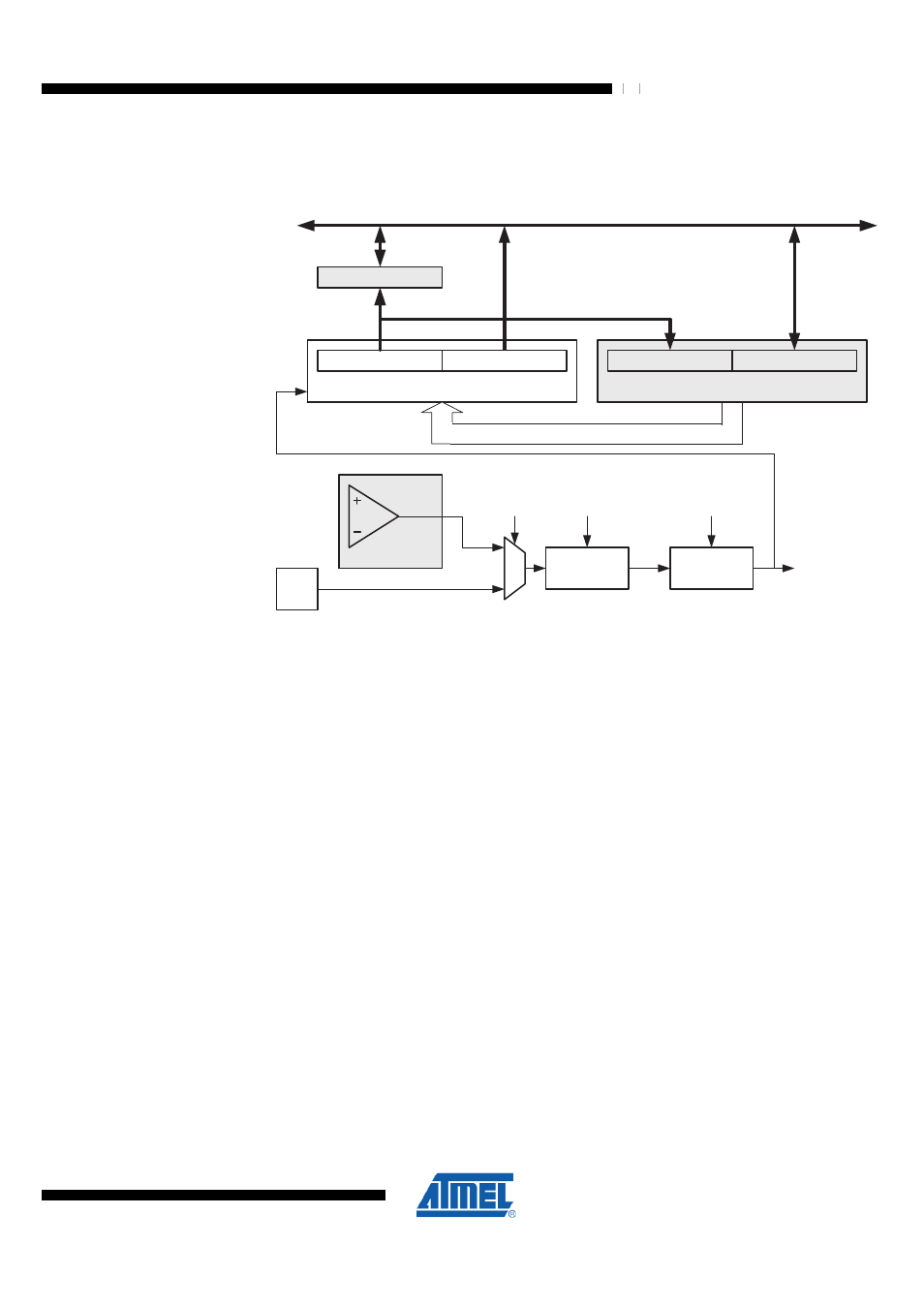
Figure 18-3. Input Capture Unit Block Diagram
ICFn (Int.Req.)
Analog
Comparator
WRITE
ICRn (16-bit Register)
ICRnH (8-bit)
Noise
Canceler
ICPn
Edge
Detector
TEMP (8-bit)
DATA BUS
(8-bit)
ICRnL (8-bit)
TCNTn (16-bit Counter)
TCNTnH (8-bit)
TCNTnL (8-bit)
ACIC*
ICNC
ICES
ACO*
Note:
1. The Analog Comparator Output (ACO) can only trigger the Timer/Counter1 ICP –
not Timer/Counter3, 4 or 5.
Reading the 16-bit value in the Input Capture Register (ICRn) is done by first reading
the low byte (ICRnL) and then the high byte (ICRnH). When the low byte is read the
high byte is copied into the high byte Temporary Register (TEMP). The CPU will access
the TEMP Register when reading the ICRnH I/O location.
The ICRn Register can only be written when using a Waveform Generation mode that
utilizes the ICRn Register for defining the counter’s TOP value. In these cases the
Waveform Generation mode (WGMn3:0) bits must be set before the TOP value can be
written to the ICRn Register. When writing the ICRn Register the high byte must be
written to the ICRnH I/O location before the low byte is written to ICRnL.
For more information on how to access the 16-bit registers refer to
.
18.6.1 Input Capture Trigger Source
The main trigger source for the input capture unit is the Input Capture Pin (ICPn).
Timer/Counter1 can alternatively use the analog comparator output as trigger source for
the input capture unit. The Analog Comparator is selected as trigger source by setting
the analog Comparator Input Capture (ACIC) bit in the Analog Comparator Control and
Status Register (ACSR). Be aware that changing trigger source can trigger a capture.
The input capture flag must therefore be cleared after the change.
Both the Input Capture Pin (ICPn) and the Analog Comparator output (ACO) inputs are
sampled using the same technique as for the Tn pin (
). The
edge detector is also identical. However, when the noise canceller is enabled,
additional logic is inserted before the edge detector increasing the delay by four system