3 eeprom data memory, 1 eeprom read write access, Atmega128rfa1 – Rainbow Electronics ATmega128RFA1 User Manual
Page 20
20
8266A-MCU Wireless-12/09
ATmega128RFA1
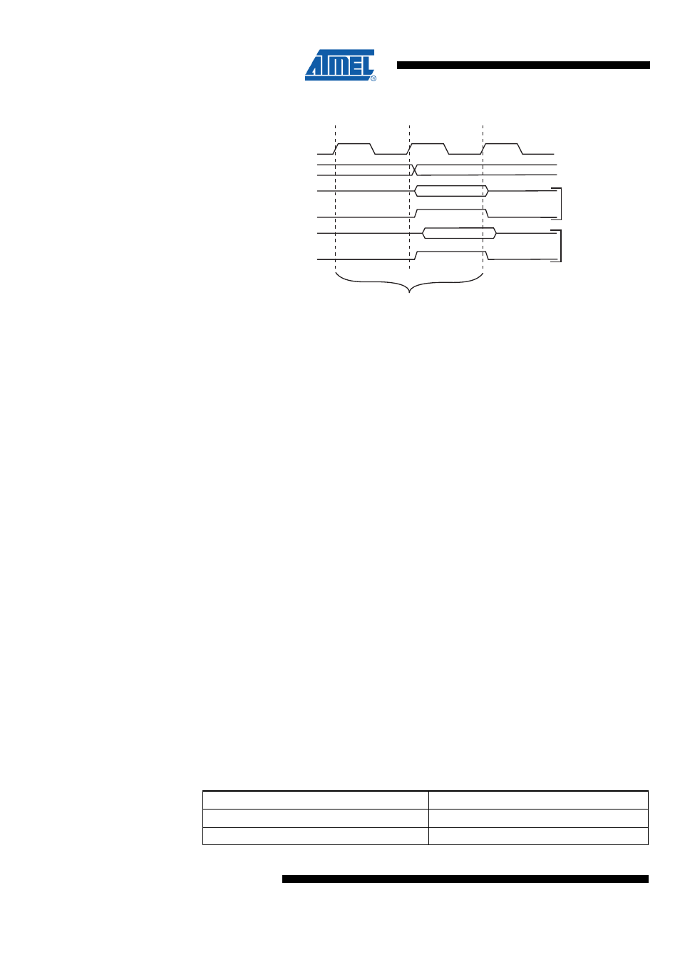
Figure 8-8. On-Chip Data SRAM Access Cycles
clk
WR
RD
Data
Data
Address
Address valid
T1
T2
T3
Compute Address
Read
Wr
ite
CPU
Memory Access Instruction
Next Instruction
8.3 EEPROM Data Memory
The ATmega128RFA1 contains 4Kbyte of data EEPROM memory. It is organized as a
separate data space, in which single bytes can be read and written. The EEPROM has
an endurance of at least 2000 write/erase cycles. The access between the EEPROM
and the CPU is described in the following, specifying the EEPROM Address Registers,
the EEPROM Data Register, and the EEPROM Control Register.
For a detailed description of SPI, JTAG and Parallel data downloading to the EEPROM,
see
"Serial Downloading" on page 477
"Programming via the JTAG Interface" on page
"Programming the EEPROM" on page 491
8.3.1 EEPROM Read Write Access
The EEPROM Access Registers are accessible in the I/O space, see
Register Description" on page 23
.
The write access time for the EEPROM is given in
. A self-timing
function, however, lets the user software detect when the next byte can be written. If the
user code contains instructions that write the EEPROM, some precautions must be
taken. In heavily filtered power supplies, DVDD is likely to rise or fall slowly on power-
up/down. This causes the device for some period of time to run at a voltage lower than
specified as minimum for the clock frequency used. See
for details on how to avoid problems in these situations.
In order to prevent unintentional EEPROM writes, a specific write procedure must be
followed. See the description of the EEPROM Control Register for details on this,
"EEPROM Register Description" on page 23
.
When the EEPROM is read, the CPU is halted for four clock cycles before the next
instruction is executed. When the EEPROM is written, the CPU is halted for two clock
cycles before the next instruction is executed.
The calibrated Oscillator is used to time the EEPROM accesses. The following table
lists the typical programming time for EEPROM access from the CPU.
Table 8-3. EEPROM Programming Time
Symbol
Typical Programming time
EEPROM write (from CPU)
4ms
EEPROM erase (from CPU)
8ms