6 compare match output unit, 1 compare output mode and waveform generation, Atmega128rfa1 – Rainbow Electronics ATmega128RFA1 User Manual
Page 230
230
8266A-MCU Wireless-12/09
ATmega128RFA1
Be aware that the COM0x1:0 bits are not double buffered together with the compare
value. A Change of the COM0x1:0 bits will take effect immediately.
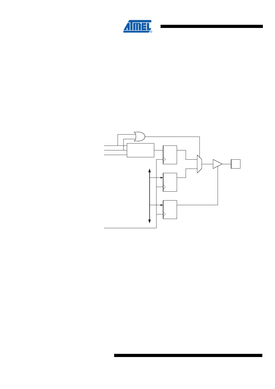
17.6 Compare Match Output Unit
The Compare Output mode (COM0x1:0) bits have two functions. The Waveform
Generator uses the COM0x1:0 bits for defining the Output Compare (OC0x) state at the
next Compare Match. The COM0x1:0 bits control also the OC0x pin output source.
Figure 17-4 shows a simplified schematic of the logic affected by the COM0x1:0 bit
setting. The I/O Registers, I/O bits and I/O pins in the figure are shown in bold. Only the
parts of the general I/O Port Control Registers (DDR and PORT) affected by the
COM0x1:0 bits are shown. When referring to the OC0x state, the reference is to the
internal OC0x Register and not to the OC0x pin. The OC0x Register is reset to “0” if a
system reset occurs.
Figure 17-4. Compare Match Output Unit Schematic
PORT
DDR
D
Q
D
Q
OCnx
Pin
OCnx
D
Q
Waveform
Generator
COMnx1
COMnx0
0
1
D
A
T
A B
US
FOCn
clk
I/O
The general I/O port function is overridden by the Output Compare (OC0x) from the
Waveform Generator if either of the COM0x1:0 bits are set. However the OC0x pin
direction (input or output) is still controlled by the Data Direction Register (DDR) of the
port pin. The Data Direction Register bit of the OC0x pin (DDR_OC0x) must be set as
output before the OC0x value is visible at the pin. The port override function is
independent of the Waveform Generation mode.
The design of the Output Compare pin logic allows initializing the OC0x state before the
output is enabled. Note that some COM0x1:0 bit settings are reserved for certain
modes of operation (see
"Register Description" on page 238
).
17.6.1 Compare Output Mode and Waveform Generation
The Waveform Generator uses the COM0x1:0 bits differently in Normal, CTC and PWM
modes. A setting of COM0x1:0 = 0 tells the Waveform Generator in all modes that no
action on the OC0x Register is to be performed on the next Compare Match. For
compare output actions in the non-PWM modes refer to Table 17-2. For fast PWM
mode refer to Table 17-3 and for phase correct PWM refer to Table 17-4.