2 alternate functions of port d, Atmega128rfa1 – Rainbow Electronics ATmega128RFA1 User Manual
Page 195
195
8266A-MCU Wireless-12/09
ATmega128RFA1
Signal
Name
PB7/OC0A/OC1C PB6/OC1B
PB5/OC1A
PB4/OC2A
PUOV
0
0
0
0
DDOE
0
0
0
0
DDOV
0
0
0
0
PVOE
OC0/OC1C
ENABLE
OC1B ENABLE
OC1A ENABLE
OC2A ENABLE
PVOV
OC0/OC1C
OC1B
OC1A
OC2A
DIEOE PCINT7•PCIE0
PCINT6•PCIE0
PCINT5•PCIE0
PCINT4•PCIE0
DIEOV 1
1
1
1
DI
PCINT7 INPUT
PCINT6 INPUT
PCINT5 INPUT
PCINT4 INPUT
AIO
–
–
–
–
Table 14-5. Overriding Signals for Alternate Functions in PB3:PB0
Signal
Name
PB3/MISO/PDO
PB2/MOSI/PDI
PB1/SCK
PB0/SS
¯ ¯
PUOE
SPE•MSTR
SPE•(~MSTR)
SPE•(~MSTR)
SPE•(~MSTR)
PUOV
PORTB3•(~PUD)
PORTB2•(~PUD)
PORTB1•(~PUD)
PORTB0•(~PUD)
DDOE
SPE•MSTR
SPE•(~MSTR)
SPE•(~MSTR)
SPE•(~MSTR)
DDOV
0
0
0
0
PVOE
SPE•(~MSTR)
SPE•MSTR
SPE•MSTR
0
PVOV
SPI SLAVE
OUTPUT
SPI MSTR
OUTPUT
SCK OUTPUT
0
DIEOE PCINT3•PCIE0
PCINT2•PCIE0
PCINT1•PCIE0
PCINT0•PCIE0
DIEOV 1
1
1
1
DI
SPI MSTR INPUT
PCINT3 INPUT
SPI SLAVE INPUT
PCINT2 INPUT
SCK INPUT
PCINT1 INPUT
SPI SS
¯ ¯ PCINT0
INPUT
AIO
–
–
–
–
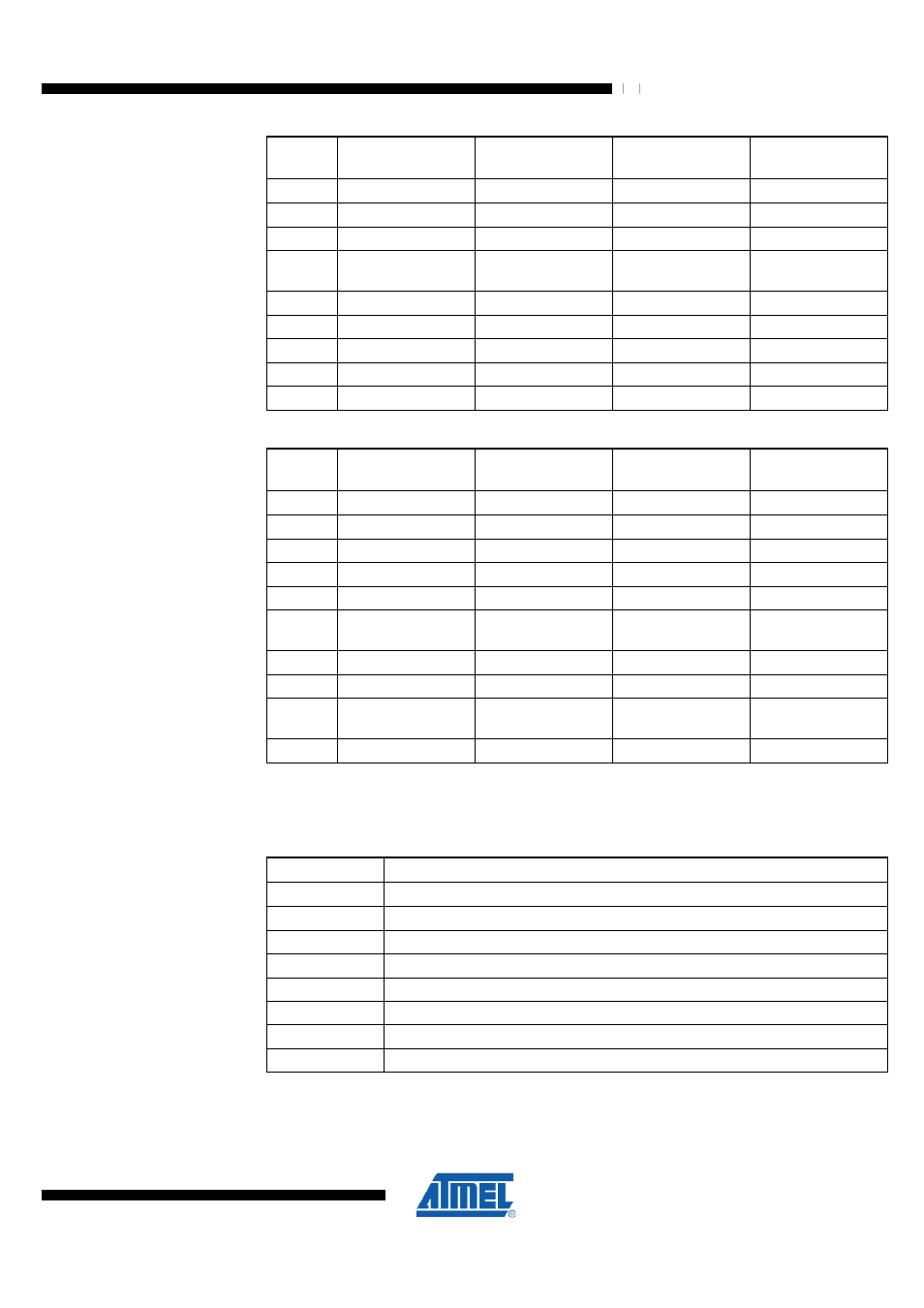
14.3.2 Alternate Functions of Port D
The Port D pins with alternate functions are shown in the following table.
Table 14-6. Port D Pins Alternate Functions
Port Pin
Alternate Function
PD7
T0 (Timer/Counter0 Clock Input)
PD6
T1 (Timer/Counter1 Clock Input)
PD5
XCK1 (USART1 External Clock Input/Output)
PD4
ICP1 (Timer/Counter1Input Capture Trigger)
PD3
INT3/TXD1 (External Interrupt3 Input or USART1 Transmit Pin)
PD2
INT2/RXD 1(External Interrupt2 Input or USART1 Receive Pin)
PD1
INT1/SDA (External Interrupt1 Input or TWI Serial Data)
PD0
INT0/SCL (External Interrupt0 Input or TWI Serial Clock)
The alternate pin configuration is as follows:
•
T0 – Port D, Bit 7
T0, this is Timer/Counter0 counter source.