8 avr memories, 1 in-system reprogrammable flash program memory, 2 sram data memory – Rainbow Electronics ATmega128RFA1 User Manual
Page 18
18
8266A-MCU Wireless-12/09
ATmega128RFA1
8 AVR Memories
This section describes the different memories in the ATmega128RFA1. The AVR
architecture has two main memory spaces, the Data Memory and the Program Memory
space. In addition, the ATmega128RFA1 features an EEPROM Memory for data
storage. All three memory spaces are linear and regular.
8.1 In-System Reprogrammable Flash Program Memory
The ATmega128RFA1 contains 128K bytes On-chip In-System Reprogrammable Flash
memory for program storage, see
. Since all AVR instructions are 16 or
32 bits wide, the Flash is 16 bit wide. For software security, the Flash Program memory
space is divided into two sections, Boot Program section and Application Program
section.
The Flash memory has an endurance of at least 2000 write/erase cycles. The
ATmega128RFA1 Program Counter (PC) is 16 bits wide, thus addressing the required
program memory locations. The operation of Boot Program section and associated
Boot Lock bits for software protection are described in detail in
Read-While-Write Self-Programming" on page 450
contains a detailed description on Flash data serial downloading using the SPI pins
or the JTAG interface.
Constant tables can be allocated within the entire program memory address space (see
the LPM – Load Program Memory instruction description and ELPM – Extended Load
Program Memory instruction description).
Timing diagrams for instruction fetch and execution are presented in
.
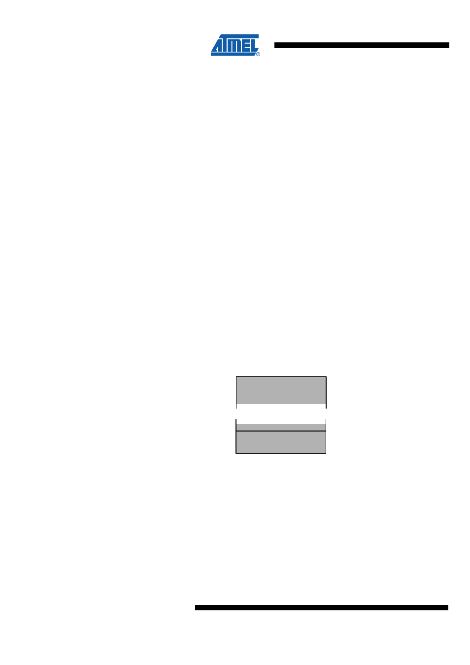
Figure 8-6. Program Flash Memory Map
Boot Flash Section
Program Memory
Application Flash Section
$0000
8.2 SRAM Data Memory
page 19 shows how the ATmega128RFA1 SRAM Memory is organized.
The ATmega128RFA1 is a complex microcontroller with more peripheral units than can
be supported within the 64 location reserved in the Opcode for the IN and OUT
instructions. For the Extended I/O space from $060 – $1FF in SRAM, only the
ST/STS/STD and LD/LDS/LDD instructions can be used.
The first Data Memory locations address both the Register File, the I/O Memory,
Extended I/O Memory, and the internal data SRAM. The first 32 locations address the
Register file, the next 64 location the standard I/O Memory, then 416 locations of
Extended I/O memory and the following locations address the internal data SRAM.