Atmega128rfa1 – Rainbow Electronics ATmega128RFA1 User Manual
Page 106

106
8266A-MCU Wireless-12/09
ATmega128RFA1
This register bit enables pin DIG3 and pin DIG4 to indicate the transmit state of the
radio transceiver. The control of the external RF front-end is disabled when this bit is 0.
Both pins DIG3 and DIG4 are then low. The control of the external front-end is enabled
when this bit is 1. DIG3 and DIG4 then indicate the state of the radio transceiver. Pin
DIG3 is high and pin DIG4 is low in the state TX_BUSY. In all other states pin DIG3 is
low and pin DIG4 is high. It is recommended to set PA_EXT_EN=1 only in receive or
transmit states to reduce the power consumption or avoid leakage current of external
RF switches or other building blocks especially during SLEEP state.
•
Bit 6 – IRQ_2_EXT_EN - Connect Frame Start IRQ to TC1
When this bit is set to one the capture input of Timer/Counter 1 is connected to the RX
frame start signal and pin DIG2 becomes an output, driving the RX frame start signal.
Antenna Diversity RF switch control (ANT_EXT_SW_EN=1) shall not be used at the
same time, because it shares the same device pin. The function IRQ_2_EXT_EN is
available for alternate frame time stamping using Timer/Counter 1. In general the
preferred method for frame time stamping is using the symbol counter.
•
Bit 5 – TX_AUTO_CRC_ON - Enable Automatic CRC Calculation
This register bit controls the automatic FCS generation for TX operations. The
automatic FCS algorithm is performed autonomously by the radio transceiver if register
bit TX_AUTO_CRC_ON=1.
•
Bit 4:0 – Res4:0 - Reserved
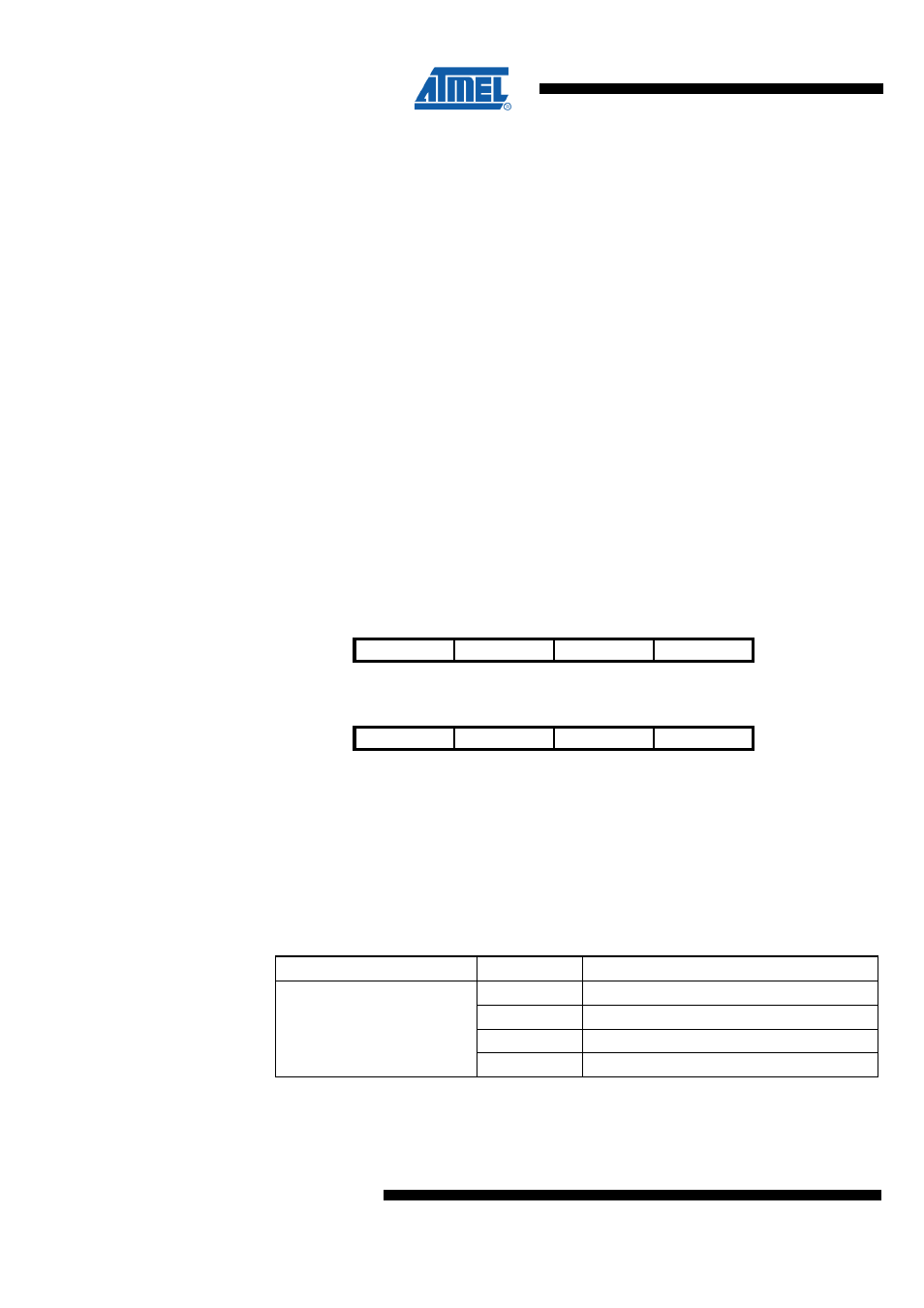
9.12.9 PHY_TX_PWR – Transceiver Transmit Power Control Register
Bit
7
6
5
4
NA ($145)
PA_BUF_LT1
PA_BUF_LT0
PA_LT1
PA_LT0
PHY_TX_PWR
Read/Write
RW
RW
RW
RW
Initial Value
1
1
0
0
Bit
3
2
1
0
NA ($145)
TX_PWR3
TX_PWR2
TX_PWR1
TX_PWR0
PHY_TX_PWR
Read/Write
RW
RW
RW
RW
Initial Value
0
0
0
0
This register controls the output power and the ramping of the transmitter.
•
Bit 7:6 – PA_BUF_LT1:0 - Power Amplifier Buffer Lead Time
These register bits control the enable lead time of the internal PA buffer relative to the
enable time of the internal PA. This time is further used to derive a control signal for an
external RF front-end to switch between receive and transmit.
Table 9-36 PA_BUF_LT Register Bits
Register Bits
Value
Description
0
0 µs
1
2 µs
2
4 µs
PA_BUF_LT1:0
3
6 µs
•
Bit 5:4 – PA_LT1:0 - Power Amplifier Lead Time
These register bits control the enable lead time of the internal power amplifier relative to
the beginning of the transmitted frame (SHR).
