11 register description, 1 admux - adc multiplexer selection register, Atmega128rfa1 – Rainbow Electronics ATmega128RFA1 User Manual
Page 427
427
8266A-MCU Wireless-12/09
ATmega128RFA1
Parameter
Register
Recommended Setup
ADCSRB
MUX5 = 1;
ADC Clock
ADCSRA
Select a clock frequency of 500kHz or lower;
V
REF
ADMUX
Select the internal 1.6V reference voltage;
Start-up time
ADCSRC
Standard requirement of 20µs is sufficient;
Tracking time
ADCSRC
Setting ADTHT = 0 is sufficient;
The A/D conversion result will always be a positive number for both V
DRTBBP
and
V
DRTBBN
. The SRAM supply voltage is easily calculated according to the following
equation (see chapter
"SRAM with Data Retention" on page 163
):
)
(
,
,
DRTBBN
DRTBBP
DD
DRT
SRAM
DD
V
V
V
V
+
−
=
The conversion result is coded as described in
with a GAIN of 0.5. It is not possible to read both V
DRTBBP
and V
DRTBBN
at the same time.
However the time required for the A/D conversion is short compared to the time
constant of a DRT voltage change.
27.11 Register Description
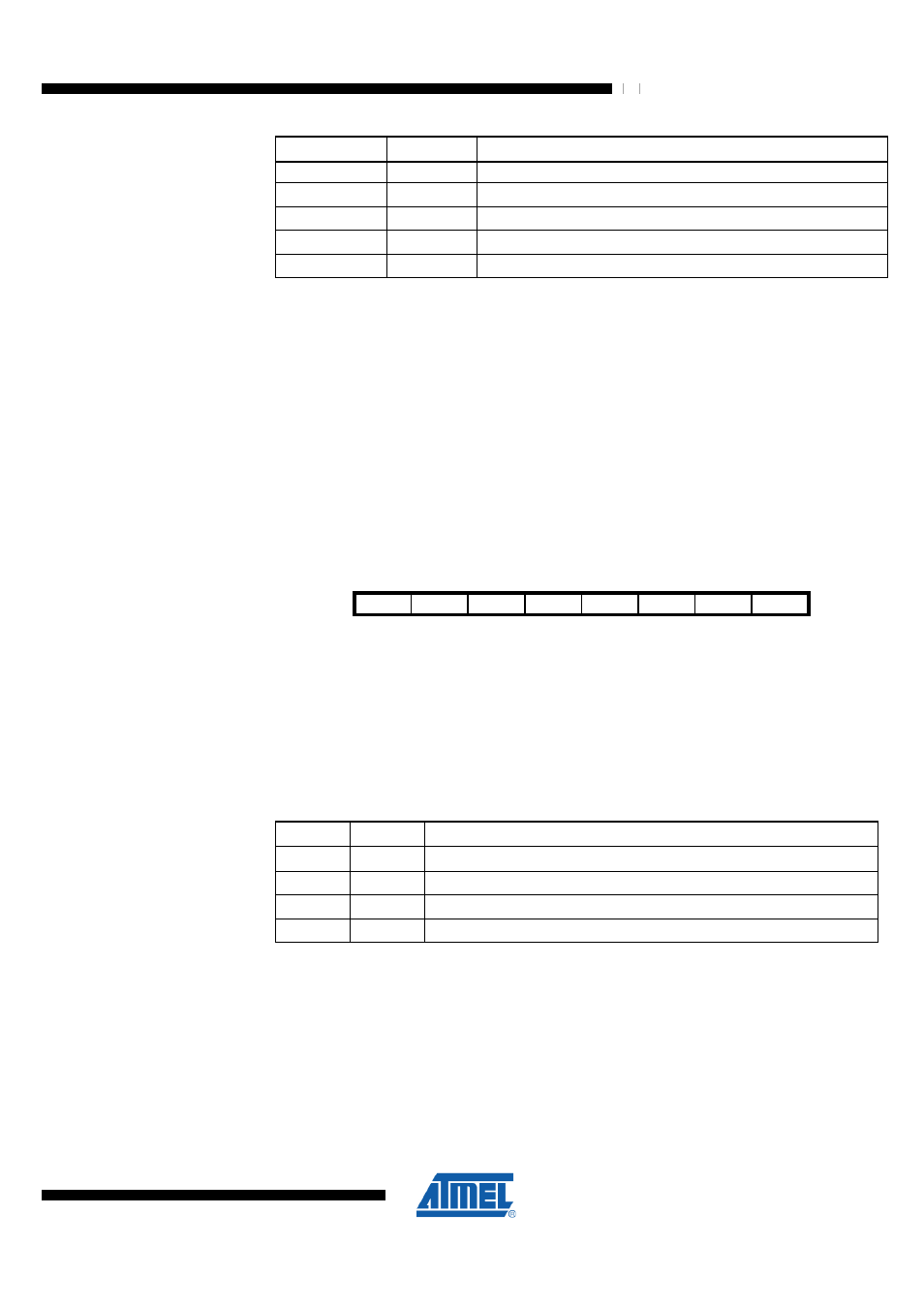
27.11.1 ADMUX – ADC Multiplexer Selection Register
Bit
7
6
5
4
3
2
1
0
NA ($7C)
REFS1
REFS0
ADLAR
MUX4
MUX3
MUX2
MUX1
MUX0
ADMUX
Read/Write
RW
RW
RW
RW
RW
RW
RW
RW
Initial Value
0
0
0
0
0
0
0
0
•
Bit 7:6 – REFS1:0: Reference Selection Bits
These bits select the voltage reference for the ADC, as shown in the following table.
Changes of these bits will only take effect until the first conversion start is requested by
setting ADSC. After this the ADC has to be disabled and enabled again for new
reference selections. The internal voltage reference options may not be used if an
external reference voltage is being applied to the AREF pin.
Table 27-10. Reference Voltage Selections for ADC
REFS1
REFS0
Reference Voltage Selection
0
0
AREF, Internal V
REF
turned off
0
1
AVDD (1.8V)
1
0
Internal 1.5V Voltage Reference (no external capacitor at AREF pin)
1
1
Internal 1.6V Voltage Reference (no external capacitor at AREF pin)
•
Bit 5 – ADLAR: ADC Left Adjust Result
The ADLAR bit affects the presentation of the A/D conversion result in the ADC Data
Register. Write one to ADLAR to left adjust the result. Otherwise, the result is right
adjusted. Changing the ADLAR bit will affect the ADC Data Register immediately,
regardless of any ongoing conversions. For a complete description of this bit, see
"ADCL and ADCH – The ADC Data Register" on page 432
.
•
Bits 4:0 – MUX4:0: Analog Channel and Gain Selection Bits
The value of these bits selects which combination of analog inputs is connected to the
ADC. See
for details. If these bits are changed during a
conversion, the change will not go in effect until this conversion is complete (ADIF in