2 ports as general digital i/o, 1 configuring the port, 2 configuring the pin – Rainbow Electronics ATmega128RFA1 User Manual
Page 187: Ports as general digital i/o
187
8266A-MCU Wireless-12/09
ATmega128RFA1
14.2 Ports as General Digital I/O
The ports are bi-directional I/O ports with optional internal pull-ups.
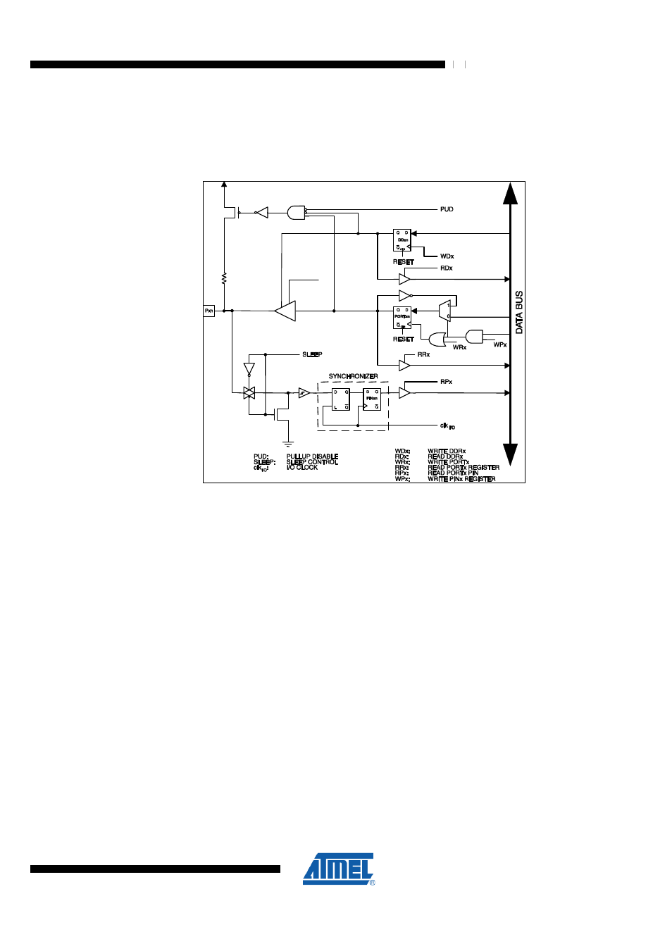
shows a functional description of one I/O-port pin, here generically called Pxn.
Figure 14-2. General Digital I/O
(1)
DPDS0/DPDS1
DPDS0/DPDS1: drive strength register
Note:
1. WRx, WPx, WDx, RRx, RPx, and RDx are common to all pins within the same port.
clk
I/O
, SLEEP, and PUD are common to all ports.
14.2.1 Configuring the Port
Drive strength of output buffers is configurable port-wise. Source/sink capably of 2mA,
4mA, 6mA or 8mA is selectable through registers DPDS1 and DPDS0. Note that pins
PG3 and PG4 of PORTG have fixed drive strength of 2mA to enable the operation of
the low power crystal oscillator.
14.2.2 Configuring the Pin
Each port pin consists of three register bits: DDxn, PORTxn, and PINxn. The DDxn bits
are accessed at the DDRx I/O address, the PORTxn bits at the PORTx I/O address,
and the PINxn bits at the PINx I/O address.
The DDxn bit in the DDRx Register selects the direction of this pin. If DDxn is written
logic one, Pxn is configured as an output pin. If DDxn is written logic zero, Pxn is
configured as an input pin.
If PORTxn is written logic one when the pin is configured as an input pin, the pull-up
resistor is activated. To switch the pull-up resistor off, PORTxn has to be written logic
zero or the pin has to be configured as an output pin. The port pins are tri-stated when
reset condition becomes active, even if no clocks are running.
If PORTxn is written logic one when the pin is configured as an output pin, the port pin
is driven high (one). If PORTxn is written logic zero when the pin is configured as an
output pin, the port pin is driven low (zero).