3 tccr2a - timer/counter2 control register a, Atmega128rfa1 – Rainbow Electronics ATmega128RFA1 User Manual
Page 325
325
8266A-MCU Wireless-12/09
ATmega128RFA1
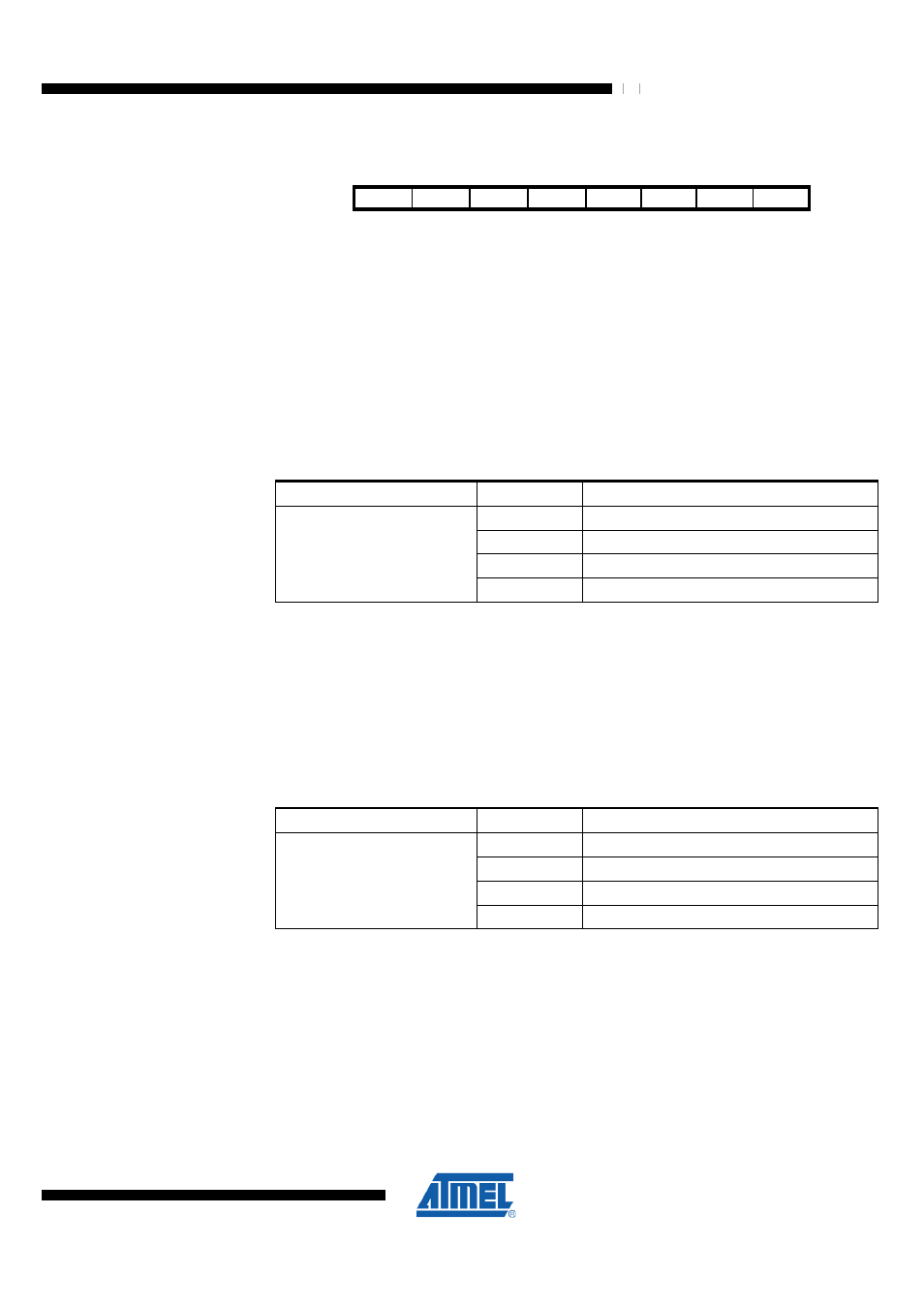
21.11.3 TCCR2A – Timer/Counter2 Control Register A
Bit
7
6
5
4
3
2
1
0
NA ($B0)
COM2A1 COM2A0 COM2B1 COM2B0
Res1
Res0
WGM21 WGM20
TCCR2A
Read/Write
RW
RW
RW
RW
RW
RW
RW
RW
Initial Value
0
0
0
0
0
0
0
0
•
Bit 7:6 – COM2A1:0 - Compare Match Output A Mode
These bits control the Output Compare pin (OC2A) behavior. If one or both of the
COM2A1:0 bits are set, the OC2A output overrides the normal port functionality of the
I/O pin it is connected to. However, note that the Data Direction Register (DDR) bit
corresponding to the OC2A pin must be set in order to enable the output driver. When
OC2A is connected to the pin, the function of the COM2A1:0 bits depends on the
WGM22:0 bit setting. The following table shows the COM2A1:0 bit functionality when
the WGM22:0 bits are set to a normal or CTC mode (non-PWM). Refer to section
"Compare Match Output Unit" for a description of the functionality in the other modes.
Table 21-7 COM2A Register Bits
Register Bits
Value
Description
0
Normal port operation, OC2A disconnected
1
Toggle OC2A on Compare Match
2
Clear OC2A on Compare Match
COM2A1:0
3
Set OC2A on Compare Match
•
Bit 5:4 – COM2B1:0 - Compare Match Output B Mode
These bits control the Output Compare pin (OC2B) behavior. If one or both of the
COM2B1:0 bits are set, the OC2B output overrides the normal port functionality of the
I/O pin it is connected to. However, note that the Data Direction Register (DDR) bit
corresponding to the OC2B pin must be set in order to enable the output driver. When
OC2B is connected to the pin, the function of the COM2B1:0 bits depends on the
WGM22:0 bit setting. The following table shows the COM2B1:0 bit functionality when
the WGM22:0 bits are set to a normal or CTC mode (non-PWM). Refer to section
"Compare Match Output Unit" for a description of the functionality in the other modes.
Table 21-8 COM2B Register Bits
Register Bits
Value
Description
0
Normal port operation, OC2B disconnected
1
Toggle OC2B on Compare Match
2
Clear OC2B on Compare Match
COM2B1:0
3
Set OC2B on Compare Match
•
Bit 3:2 – Res1:0 - Reserved
•
Bit 1:0 – WGM21:20 - Waveform Generation Mode
Combined with the WGM22 bit found in the TCCR2B Register, these bits control the
counting sequence of the counter, the source for maximum (TOP) counter value, and
what type of waveform generation to be used. Modes of operation supported by the
Timer/Counter2 unit are: Normal mode (counter), Clear Timer on Compare Match
(CTC) mode, and two types of Pulse Width Modulation (PWM) modes (see section
"Modes of Operation" for details).