Atmega128rfa1 – Rainbow Electronics ATmega128RFA1 User Manual
Page 500
500
8266A-MCU Wireless-12/09
ATmega128RFA1
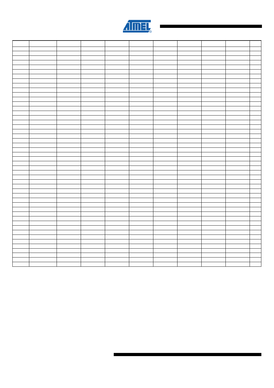
Address
Name
Bit 7
Bit 6
Bit 5
Bit 4
Bit 3
Bit 2
Bit 1
Bit 0
Page
...
Reserved
0x2E (0x4E)
SPDR
SPDR7
SPDR6
SPDR5
SPDR4
SPDR3
SPDR2
SPDR1
SPDR0
0x2D (0x4D)
SPSR
SPIF
WCOL
Res4
Res3
Res2
Res1
Res0
SPI2X
0x2C (0x4C)
SPCR
SPIE
SPE
DORD
MSTR
CPOL
CPHA
SPR1
SPR0
0x2B (0x4B)
GPIOR2
GPIOR27
GPIOR26
GPIOR25
GPIOR24
GPIOR23
GPIOR22
GPIOR21
GPIOR20
0x2A (0x4A)
GPIOR1
GPIOR17
GPIOR16
GPIOR15
GPIOR14
GPIOR13
GPIOR12
GPIOR11
GPIOR10
...
Reserved
0x28 (0x48)
OCR0B
OCR0B_7
OCR0B_6
OCR0B_5
OCR0B_4
OCR0B_3
OCR0B_2
OCR0B_1
OCR0B_0
0x27 (0x47)
OCR0A
OCR0A_7
OCR0A_6
OCR0A_5
OCR0A_4
OCR0A_3
OCR0A_2
OCR0A_1
OCR0A_0
0x26 (0x46)
TCNT0
TCNT0_7
TCNT0_6
TCNT0_5
TCNT0_4
TCNT0_3
TCNT0_2
TCNT0_1
TCNT0_0
0x25 (0x45)
TCCR0B
FOC0A
FOC0B
Res1
Res0
WGM02
CS02
CS01
CS00
0x24 (0x44)
TCCR0A
COM0A1
COM0A0
COM0B1
COM0B0
Res1
Res0
WGM01
WGM00
0x23 (0x43)
GTCCR
TSM
Res4
Res3
Res2
Res1
Res0
PSRASY
PSRSYNC
0x22 (0x42)
EEARH
Res3
Res2
Res1
Res0
EEAR11
EEAR10
EEAR9
EEAR8
0x21 (0x41)
EEARL
EEAR7
EEAR6
EEAR5
EEAR4
EEAR3
EEAR2
EEAR1
EEAR0
0x20 (0x40)
EEDR
EEDR7
EEDR6
EEDR5
EEDR4
EEDR3
EEDR2
EEDR1
EEDR0
0x1F (0x3F)
EECR
Res1
Res0
EEPM1
EEPM0
EERIE
EEMPE
EEPE
EERE
0x1E (0x3E)
GPIOR0
GPIOR07
GPIOR06
GPIOR05
GPIOR04
GPIOR03
GPIOR02
GPIOR01
GPIOR00
0x1D (0x3D)
EIMSK
INT7
INT6
INT5
INT4
INT3
INT2
INT1
INT0
0x1C (0x3C)
EIFR
INTF7
INTF6
INTF5
INTF4
INTF3
INTF2
INTF1
INTF0
0x1B (0x3B)
PCIFR
Res4
Res3
Res2
Res1
Res0
PCIF2
PCIF1
PCIF0
0x1A (0x3A)
TIFR5
Res1
Res0
ICF5
Res
OCF5C
OCF5B
OCF5A
TOV5
0x19 (0x39)
TIFR4
Res1
Res0
ICF4
Res
OCF4C
OCF4B
OCF4A
TOV4
0x18 (0x38)
TIFR3
Res1
Res0
ICF3
Res
OCF3C
OCF3B
OCF3A
TOV3
0x17 (0x37)
TIFR2
Res4
Res3
Res2
Res1
Res0
OCF2B
OCF2A
TOV2
0x16 (0x36)
TIFR1
Res1
Res0
ICF1
Res
OCF1C
OCF1B
OCF1A
TOV1
0x15 (0x35)
TIFR0
Res4
Res3
Res2
Res1
Res0
OCF0B
OCF0A
TOV0
0x14 (0x34)
PORTG
Res1
Res0
PORTG5
PORTG4
PORTG3
PORTG2
PORTG1
PORTG0
0x13 (0x33)
DDRG
Res1
Res0
DDG5
DDG4
DDG3
DDG2
DDG1
DDG0
0x12 (0x32)
PING
Res1
Res0
PING5
PING4
PING3
PING2
PING1
PING0
0x11 (0x31)
PORTF
PORTF7
PORTF6
PORTF5
PORTF4
PORTF3
PORTF2
PORTF1
PORTF0
0x10 (0x30)
DDRF
DDF7
DDF6
DDF5
DDF4
DDF3
DDF2
DDF1
DDF0
0x0F (0x2F)
PINF
PINF7
PINF6
PINF5
PINF4
PINF3
PINF2
PINF1
PINF0
0x0E (0x2E)
PORTE
PORTE7
PORTE6
PORTE5
PORTE4
PORTE3
PORTE2
PORTE1
PORTE0
0x0D (0x2D)
DDRE
DDE7
DDE6
DDE5
DDE4
DDE3
DDE2
DDE1
DDE0
0x0C (0x2C)
PINE
PINE7
PINE6
PINE5
PINE4
PINE3
PINE2
PINE1
PINE0
0x0B (0x2B)
PORTD
PORTD7
PORTD6
PORTD5
PORTD4
PORTD3
PORTD2
PORTD1
PORTD0
0x0A (0x2A)
DDRD
DDD7
DDD6
DDD5
DDD4
DDD3
DDD2
DDD1
DDD0
0x09 (0x29)
PIND
PIND7
PIND6
PIND5
PIND4
PIND3
PIND2
PIND1
PIND0
0x08 (0x28)
PORTC
PORTC7
PORTC6
PORTC5
PORTC4
PORTC3
PORTC2
PORTC1
PORTC0
0x07 (0x27)
DDRC
DDC7
DDC6
DDC5
DDC4
DDC3
DDC2
DDC1
DDC0
0x06 (0x26)
PINC
PINC7
PINC6
PINC5
PINC4
PINC3
PINC2
PINC1
PINC0
0x05 (0x25)
PORTB
PORTB7
PORTB6
PORTB5
PORTB4
PORTB3
PORTB2
PORTB1
PORTB0
0x04 (0x24)
DDRB
DDB7
DDB6
DDB5
DDB4
DDB3
DDB2
DDB1
DDB0
0x03 (0x23)
PINB
PINB7
PINB6
PINB5
PINB4
PINB3
PINB2
PINB1
PINB0
0x02 (0x22)
PORTA
PORTA7
PORTA6
PORTA5
PORTA4
PORTA3
PORTA2
PORTA1
PORTA0
0x01 (0x21)
DDRA
DDA7
DDA6
DDA5
DDA4
DDA3
DDA2
DDA1
DDA0
0x00 (0x20)
PINA
PINA7
PINA6
PINA5
PINA4
PINA3
PINA2
PINA1
PINA0
Notes:
1. Reserved registers, bits and I/O memory addresses (marked as Res*) may not be modified.
2. I/O registers within the address range 0x00 - 0x1F are directly bit-accessible using the SBI and CBI instructions. In these registers, the
value of single bits can be checked by using the SBIS and SBIC instructions.
3. Some of the status flags are cleared by writing a logical one to them. Note that the CBI and SBI instructions will operate on all bits in the
I/O register, writing a one back into any flag read as set, thus clearing the flag. The CBI and SBI instructions work with registers 0x00 to
0x1F only.
4. When using the I/O specific commands IN and OUT, the I/O addresses 0x00 – 0x3F must be used. When addressing I/O registers as
data space using LD and ST instructions, 0x20 must be added to these addresses. The device is a complex microcontroller with more
peripheral units than can be supported within the 64 location reserved in Op-code for the IN and OUT instructions. For the Extended I/O
space from 0x60 – 0x1FF in SRAM, only the ST/STS/STD and LD/LDS/LDD instructions can be used.