16 trx_ctrl_2 - transceiver control register 2, 17 ant_div - antenna diversity control register, Atmega128rfa1 – Rainbow Electronics ATmega128RFA1 User Manual
Page 112
112
8266A-MCU Wireless-12/09
ATmega128RFA1
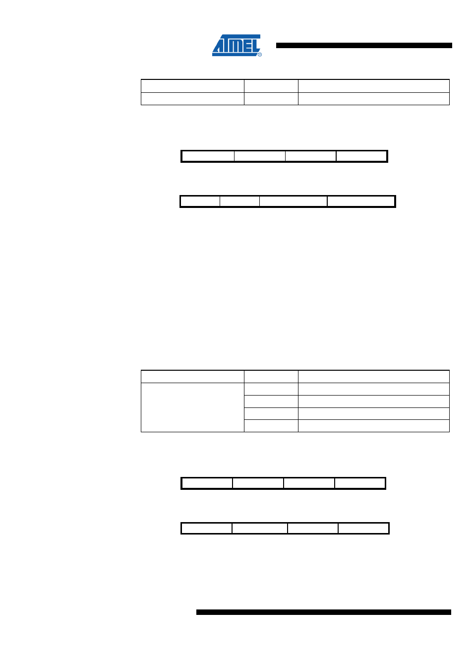
Table 9-45 SFD_VALUE Register Bits
Register Bits
Value
Description
SFD_VALUE7:0
0xA7
IEEE 802.15.4 compliant value of the SFD
9.12.16 TRX_CTRL_2 – Transceiver Control Register 2
Bit
7
6
5
4
NA ($14C)
RX_SAFE_MODE
Res4
Res3
Res2
TRX_CTRL_2
Read/Write
RW
R
R
R
Initial Value
0
0
0
0
Bit
3
2
1
0
NA ($14C)
Res1
Res0
OQPSK_DATA_RATE1 OQPSK_DATA_RATE0
TRX_CTRL_2
Read/Write
R
R
RW
RW
Initial Value
0
0
0
0
This register controls the data rate setting of the radio transceiver.
•
Bit 7 – RX_SAFE_MODE - RX Safe Mode
If this bit is set, the next received frame will be protected and not overwritten by
following frames. Set this bit to 0 to release the buffer (and set it again for further
protection).
•
Bit 6:2 – Res4:0 - Reserved
•
Bit 1:0 – OQPSK_DATA_RATE1:0 - Data Rate Selection
A write access to these register bits sets the OQPSK PSDU data rate used by the radio
transceiver. The reset value OQPSK_DATA_RATE = 0 is the PSDU data rate according
to IEEE 802.15.4. All other values are used in High Data Rate Modes.
Table 9-46 OQPSK_DATA_RATE Register Bits
Register Bits
Value
Description
0
250 kb/s (IEEE 802.15.4 compliant)
1
500 kb/s
2
1000 kb/s
OQPSK_DATA_RATE1:0
3
2000 kb/s
9.12.17 ANT_DIV – Antenna Diversity Control Register
Bit
7
6
5
4
NA ($14D)
ANT_SEL
Res2
Res1
Res0
ANT_DIV
Read/Write
R
R
R
R
Initial Value
0
0
0
0
Bit
3
2
1
0
NA ($14D)
ANT_DIV_EN
ANT_EXT_SW_EN
ANT_CTRL1
ANT_CTRL0
ANT_DIV
Read/Write
RW
RW
RW
RW
Initial Value
0
0
1
1
This register controls the Antenna Diversity.
•
Bit 7 – ANT_SEL - Antenna Diversity Antenna Status