34 electrical characteristics, 1 absolute maximum ratings, 1 recommended operating range – Rainbow Electronics ATmega128RFA1 User Manual
Page 501: 2 digital pin characteristics, Electrical, Atmega128rfa1
501
8266A-MCU Wireless-12/09
ATmega128RFA1
34 Electrical Characteristics
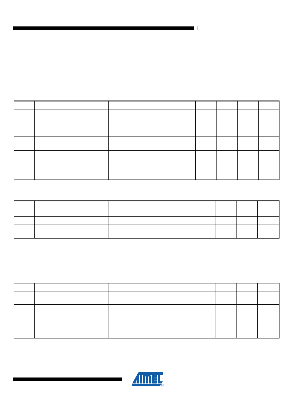
34.1 Absolute Maximum Ratings
Note that stresses beyond those listed under “Absolute Maximum Ratings” may cause
permanent damage to the device. This is a stress rating only and functional operation of
the device at these or any other conditions beyond those indicated in the operational
sections of this specification are not implied. Exposure to absolute maximum rating
conditions for extended periods may affect device reliability.
Symbol Parameter
Condition
Min.
Typ.
Max.
Units
T
STOR
Storage temperature
-50
150
°C
T
LEAD
Lead temperature
T = 10s,
(soldering profile compliant with
IPC/JEDEC J-STD-020B)
260
°C
V
ESD
ESD robustness
Compl. to [3],
Compl. to [4]
4
750
kV
V
P
RF
Input RF level
+14
dBm
V
DIG
Voltage on all pins
(except pins 4, 5, 13, 14, 29)
-0.3
V
DD
+0.3 V
V
ANA
Voltage on pins 4, 5, 13, 14, 29
-0.3
2.0
V
34.1.1 Recommended Operating Range
Symbol Parameter
Condition
Min.
Typ.
Max.
Units
T
OP
Operating temperature range
-40
+85
°C
V
DD
Supply voltage
Voltage on pins 15,28
(2)
1.8
3.0
3.6
V
V
DD1.8
Supply voltage
(on pins 13, 14, 29)
External voltage supply
(1)
1.7
1.8
1.9
V
Notes:
1. Register VREG_CTRL needs to be programmed to disable internal voltage regulators and supply blocks by an external
"Voltage Regulators (AVREG, DVREG)" on page 163
2. Even if an implementation uses the external 1.8V voltage supply V
DD1.8
it is required to connect V
DD
.
34.1.2 Digital Pin Characteristics
Test Conditions: T
OP
= 25°C (unless otherwise stated)
Symbol Parameter
Condition
Min
Typ
Max
Units
V
IH
High level input voltage
(1)
V
DD
–
0.4
V
V
IL
Low level input voltage
(1)
0.4
V
V
OH
High level output voltage
(1)
For all output driver strengths defined in
DPDS0, DPDS1
V
DD
–
0.4
V
V
OL
Low level output voltage
(1)
For all output driver strengths defined in
DPDS0, DPDS1
0.4
V
Note:
5. The capacitive load should not be larger than 50 pF for all I/Os when using the default driver strength settings, refer to
section
"DPDS0 – Port Driver Strength Register 0" on page 174
"DPDS1 – Port Driver Strength Register 1" on
page 175
. Generally, large load capacitances increase the overall current consumption.