Figure 31-14 on, Atmega128rfa1 – Rainbow Electronics ATmega128RFA1 User Manual
Page 480
480
8266A-MCU Wireless-12/09
ATmega128RFA1
Instruction Format
(1)
Read Fuse Bits
$50
$00
$00
data byte out
Read Fuse High Bits
$58
$08
$00
data byte out
Read Extended Fuse Bits
$50
$08
$00
data byte out
Read Calibration Byte
$38
$00
$00
data byte out
Write Instructions
(2)(3)
Write Program Memory Page
$4C
addr. MSB
addr. LSB
$00
Write EEPROM Memory
$C0
0000 aaaa
aaaa aaaa
data byte in
Write EEPROM Memory Page (page access)
$C2
0000 aaaa
aaaa 00
$00
Write Lock Bits
$AC
$E0
$00
data byte in
Write Fuse Bits
$AC
$A0
$00
data byte in
Write Fuse High Bits
$AC
$A8
$00
data byte in
Write Extended Fuse Bits
$AC
$A4
$00
data byte in
Notes:
1. a = address.
2. Bits are programmed ‘0’, un-programmed ‘1’.
3. To ensure future compatibility, unused Fuses and Lock bits should be un-programmed (‘1’).
4. Refer to the corresponding section for Fuse and Lock bits, Calibration and Signature bytes and Page size.
5. See http://www.atmel.com/avr for Application Notes regarding programming and programmers.
If the LSB in RDY/BSY
¯ ¯ ¯ data byte out is ‘1’, a programming operation is still pending.
Wait until this bit returns ‘0’ before the next instruction is carried out. Within the same
page, the low data byte must be loaded prior to the high data byte. After data is loaded
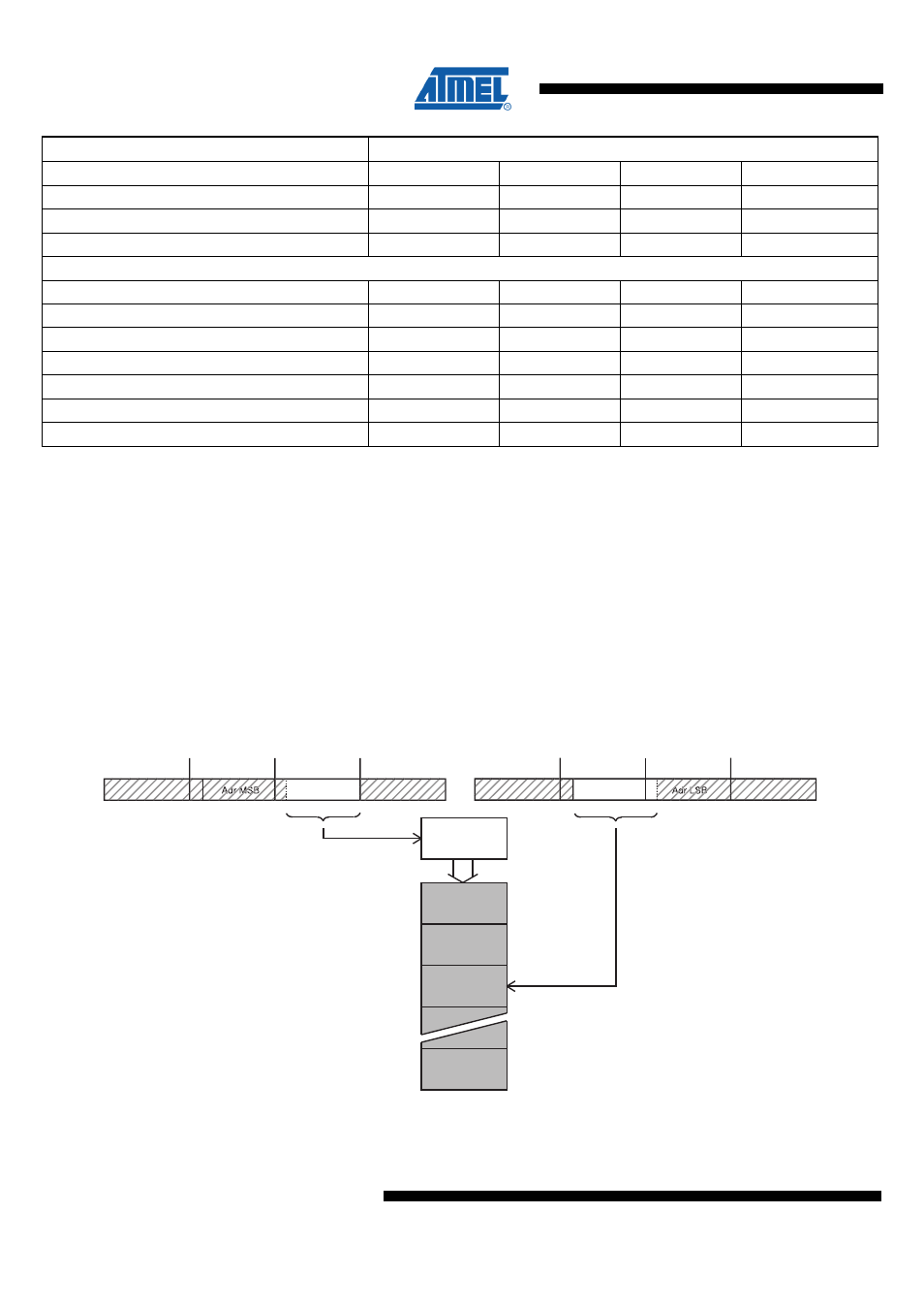
to the page buffer, program the EEPROM page; see
Figure 31-14 below
.
Figure 31-14. Serial Programming Instruction Example
Byte 1
Byte 2
Byte 3
Byte 4
Adr LSB
Bit 15 B
0
Serial Programming Instruction
Program Memory/
EEPROM Memory
Page 0
Page 1
Page 2
Page N-1
Page Buffer
Write Program Memory Page/
Write EEPROM Memory Page
Load Program Memory Page (High/Low Byte)/
Load EEPROM Memory Page (page access)
Byte 1
Byte 2
Byte 3
Byte 4
Bit 15 B
0
Adr MSB
Page Offset
Page Number
Adr MSB
Adr MSB
Adr MSB
Adr MSB
Adr MSB
Adr LSB
Adr LSB
Adr LSB
Adr LSB
Adr LSB