2 scanning the rstn, clki and tst pin, Figure 29-4 on, Atmega128rfa1 – Rainbow Electronics ATmega128RFA1 User Manual
Page 446
446
8266A-MCU Wireless-12/09
ATmega128RFA1
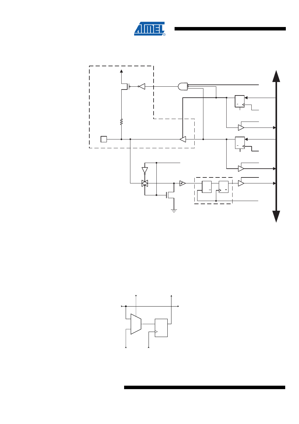
Figure 29-4. General Port Pin Schematic Diagram
CLK
RPx
RRx
WRx
RDx
WDx
PUD
SYNCHRONIZER
WDx:
WRITE DDRx
WRx:
WRITE PORTx
RRx:
READ PORTx REGISTER
RPx:
READ PORTx PIN
PUD:
PULLUP DISABLE
CLK :
I/O CLOCK
RDx:
READ DDRx
D
L
Q
Q
RESET
RESET
Q
Q
D
Q
Q
D
CLR
PORTxn
Q
Q
D
CLR
DDxn
PINxn
DA
T
A B
US
SLEEP
SLEEP:
SLEEP CONTROL
Pxn
I/O
I/O
See Boundary-scan
Description for Details!
PUExn
OCxn
ODxn
IDxn
PUExn:
PULLUP ENABLE for pin Pxn
OCxn:
OUTPUT CONTROL for pin Pxn
ODxn:
OUTPUT DATA to pin Pxn
IDxn:
INPUT DATA from pin Pxn
29.5.2 Scanning the RSTN, CLKI and TST Pin
An observe-only cell as shown in
is inserted for the active low reset
signal RSTN, for the active high programming and test mode enable signal TSTN and
for the clock input CLKI.
Figure 29-5. Observe-only Cell
0
1
D
Q
From
Previous
Cell
ClockDR
ShiftDR
To
Next
Cell
From System Pin
To System Logic
FF1
- MAX5151 (16 pages)
- MAXQ3108 (64 pages)
- MAX5661 (39 pages)
- MAX6691 (7 pages)
- MAX5362 (12 pages)
- ADC10158 (26 pages)
- MAX8922L (14 pages)
- MAX8596Z (8 pages)
- MAX7491 (18 pages)
- MAX15040 (15 pages)
- MAX5177 (16 pages)
- ADC08138 (22 pages)
- MAX5961 (42 pages)
- T89C51RD2 (86 pages)
- MAX16055 (9 pages)
- MAX6659 (17 pages)
- ADC0820 (20 pages)
- MAX6678 (19 pages)
- MAX8884Z (15 pages)
- MAX16915 (9 pages)
- MAX8620 (18 pages)
- MAX5144 (12 pages)
- MAX6670 (8 pages)
- MAX8760 (39 pages)
- W78C32C (14 pages)
- MX7533 (8 pages)
- MAX8727 (13 pages)
- MAX9053 (15 pages)
- W78C54 (16 pages)
- MAX8614B (15 pages)
- W90N740 (219 pages)
- MAX6626 (13 pages)
- ADC10738 (30 pages)
- MAX17000 (31 pages)
- MAX5051 (21 pages)
- MAXQ1004 (18 pages)
- MAX6871 (51 pages)
- MX7847 (12 pages)
- MAX6608 (6 pages)
- MAX17083 (15 pages)
- MAX6641 (17 pages)
- MAX5251 (16 pages)
- MAX6338 (8 pages)
- MAX6690 (16 pages)
- MAX8668 (18 pages)