3 tccr1c - timer/counter1 control register c, 4 tcnt1h - timer/counter1 high byte, Atmega128rfa1 – Rainbow Electronics ATmega128RFA1 User Manual
Page 270
270
8266A-MCU Wireless-12/09
ATmega128RFA1
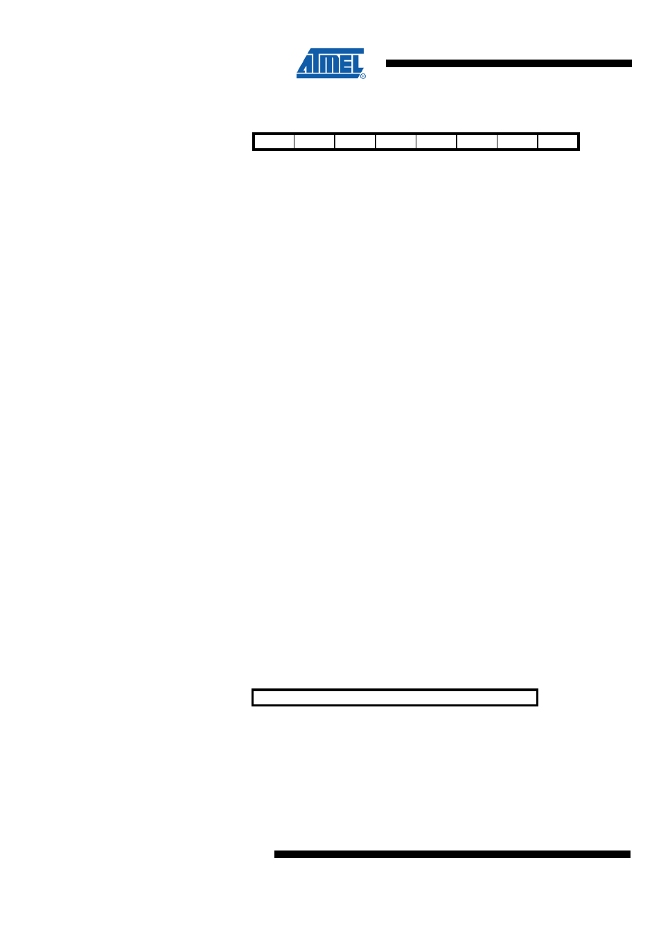
18.11.3 TCCR1C – Timer/Counter1 Control Register C
Bit
7
6
5
4
3
2
1
0
NA ($82)
FOC1A
FOC1B
FOC1C
Res4
Res3
Res2
Res1
Res0
TCCR1C
Read/Write
RW
RW
RW
R
R
R
R
R
Initial Value
0
0
0
0
0
0
0
0
•
Bit 7 – FOC1A - Force Output Compare for Channel A
The FOC1A bit is only active when the WGM13:0 bits specify a non-PWM mode. When
writing a logical one to the FOC1A bit, an immediate compare match is forced on the
waveform generation unit. The OC1A output is changed according to its COM1A1:0 bits
setting. Note that the FOC1A bits are implemented as strobes. Therefore it is the value
present in the COM1A1:0 bits that determine the effect of the forced compare. A
FOC1A strobe will not generate any interrupt nor will it clear the timer in Clear Timer on
Compare Match (CTC) mode using OCR1A as TOP. The FOC1A bits are always read
as zero.
•
Bit 6 – FOC1B - Force Output Compare for Channel B
The FOC1B bit is only active when the WGM13:0 bits specify a non-PWM mode. When
writing a logical one to the FOC1B bit, an immediate compare match is forced on the
waveform generation unit. The OC1B output is changed according to its COM1B1:0 bits
setting. Note that the FOC1B bits are implemented as strobes. Therefore it is the value
present in the COM1B1:0 bits that determine the effect of the forced compare. A
FOC1B strobe will not generate any interrupt nor will it clear the timer in Clear Timer on
Compare Match (CTC) mode using OCR1B as TOP. The FOC1B bits are always read
as zero.
•
Bit 5 – FOC1C - Force Output Compare for Channel C
The FOC1C bit is only active when the WGM13:0 bits specify a non-PWM mode. When
writing a logical one to the FOC1C bit, an immediate compare match is forced on the
waveform generation unit. The OC1C output is changed according to its COM1C1:0 bits
setting. Note that the FOC1C bits are implemented as strobes. Therefore it is the value
present in the COM1C1:0 bits that determine the effect of the forced compare. A
FOC1C strobe will not generate any interrupt nor will it clear the timer in Clear Timer on
Compare Match (CTC) mode using OCR1C as TOP. The FOC1C bits are always read
as zero.
•
Bit 4:0 – Res4:0 - Reserved
These bits are reserved for future use.
18.11.4 TCNT1H – Timer/Counter1 High Byte
Bit
7
6
5
4
3
2
1
0
NA ($85)
TCNT1H7:0
TCNT1H
Read/Write
RW
RW
RW
RW
RW
RW
RW
RW
Initial Value
0
0
0
0
0
0
0
0
The two Timer/Counter I/O locations (TCNT1H and TCNT1L, combined TCNT1) give
direct access, both for read and for write operations, to the Timer/Counter unit 16-bit
counter. To ensure that both the high and low bytes are read and written simultaneously
when the CPU accesses these registers, the access is performed using an 8-bit
temporary High Byte Register (TEMP). This temporary register is shared by all the other