1 registers, Atmega128rfa1 – Rainbow Electronics ATmega128RFA1 User Manual
Page 245
245
8266A-MCU Wireless-12/09
ATmega128RFA1
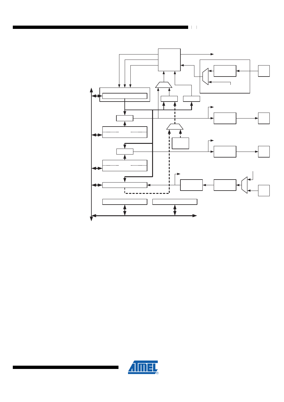
Figure 18-1. 16-bit Timer/Counter Block Diagram
(1)
Clock Select
Timer/Counter
D
A
T
A B
US
OCRnA
OCRnB
ICRn
=
=
TCNTn
Waveform
Generation
Waveform
Generation
OCnA
OCnB
Noise
Canceler
ICPn
=
Fixed
TOP
Values
Edge
Detector
Control Logic
=
0
TOP
BOTTOM
Count
Clear
Direction
TOVn
(Int.Req.)
OCnA
(Int.Req.)
OCnB
(Int.Req.)
ICFn (Int.Req.)
TCCRnA
TCCRnB
( From Analog
Comparator Ouput )
Tn
Edge
Detector
( From Prescaler )
clk
Tn
for Timer/Counter1, 2 and 3 pin placements and description.
18.2.1 Registers
The Timer/Counter (TCNTn) Output Compare Registers (OCRnA/B/C) and Input
Capture Register (ICRn) are all 16-bit registers. Special procedures must be followed
when accessing the 16-bit registers. These procedures are described in the section
"Accessing 16-bit Registers" on page 246
. The Timer/Counter Control Registers
(TCCRnA/B/C) are 8-bit registers and have no CPU access restrictions. Interrupt
requests (shorten as Int.Req.) signals are all visible in the Timer Interrupt Flag Register
(TIFRn). All interrupts are individually masked with the Timer Interrupt Mask Register
(TIMSKn). TIFRn and TIMSKn are not shown in the figure since these registers are
shared by other timer units.
The Timer/Counter can be clocked internally, via the prescaler or by an external clock
source on the Tn pin. The Clock Select logic block controls which clock source and
which clock edge the Timer/Counter uses to increment (or decrement) its value. The
Timer/Counter is inactive when no clock source is selected. The output from the clock
select logic is referred to as the timer clock (clk
Tn
).
The double buffered Output Compare Registers (OCRnA/B/C) are compared with the