3 alternate functions of port e, Atmega128rfa1 – Rainbow Electronics ATmega128RFA1 User Manual
Page 197
197
8266A-MCU Wireless-12/09
ATmega128RFA1
Signal
Name
PD7/T0
PD6/T1
PD5/XCK1
PD4/ICP1
DDOV
0
0
1
0
PVOE
0
0
XCK1 OUTPUT
ENABLE
0
PVOV
0
0
XCK1 OUTPUT
0
DIEOE
0
0
0
0
DIEOV
0
0
0
0
DI
T0 INPUT
T1 INPUT
XCK1 INPUT
ICP1 INPUT
AIO
–
–
–
–
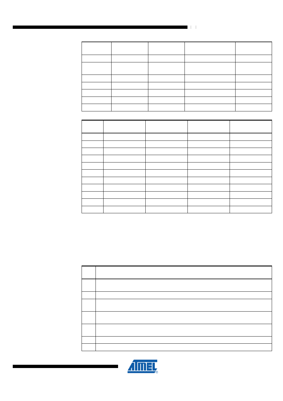
Table 14-8. Overriding Signals for Alternate Functions PD3:PD0
Signal
Name
PD3/INT3/TXD1
PD2/INT2/RXD1
PD1/INT1/SDA
PD0/INT0/SCL
PUOE
TXEN1
RXEN1
TWEN
TWEN
PUOV
0
PORTD2&(~PUD)
PORTD1&(~PUD)
PORTD0&(~PUD)
DDOE
TXEN1
RXEN1
TWEN
TWEN
DDOV
1
0
SDA_OUT
SCL_OUT
PVOE
TXEN1
0
TWEN
TWEN
PVOV
TXD1
0
0
0
DIEOE
INT3 ENABLE
INT2 ENABLE
INT1 ENABLE
INT0 ENABLE
DIEOV
1
1
1
1
DI
INT3 INPUT
INT2 INPUT/RXD1
INT1 INPUT
INT0 INPUT
AIO
-
-
SDA INPUT
SCL INPUT
Note:
1. When enabled, the 2-wire Serial Interface enables Slew-Rate controls on the
output pins PD0 and PD1. This is not shown in this table. In addition, spike filters
are connected between the AIO outputs shown in the port figure and the digital
logic of the TWI module.
14.3.3 Alternate Functions of Port E
The Port E pins with alternate functions are shown in the following table.
Table 14-9. Port E Pins Alternate Functions
Port
Pin
Alternate Function
PE7
INT7/ICP3/CLK0 (External Interrupt7 Input, Timer/Counter3 Input Capture Trigger or
Divided System Clock)
PE6
INT6/T3 (External Interrupt6 Input or Timer/Counter3 Clock Input)
PE5
INT5/OC3C (External Interrupt5 Input or Output Compare and PWM Output C for
Timer/Counter3)
PE4
INT4/OC3B (External Interrupt4 Input or Output Compare and PWM Output B for
Timer/Counter3)
PE3
AIN1/OC3A (Analog Comparator Negative Input or Output Compare and PWM Output A
for Timer/Counter3)
PE2
AIN0/XCK0 (Analog Comparator or Positive Input or USART0 external clock input/output)
PE1
TXD0 (USART0 Transmit Pin)