Rainbow Electronics ATmega128RFA1 User Manual
Page 445
445
8266A-MCU Wireless-12/09
ATmega128RFA1
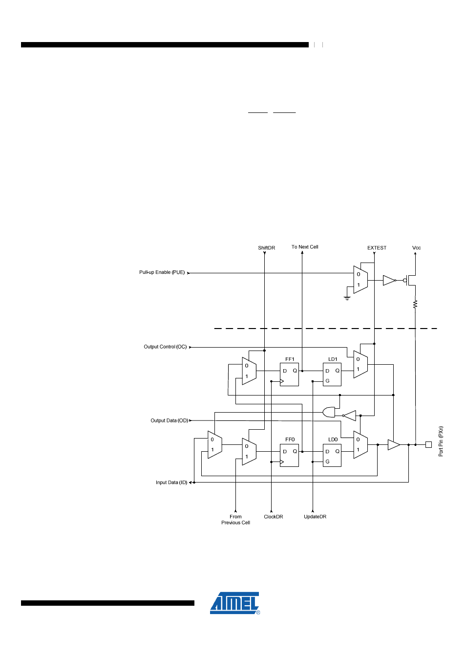
When no alternate port function is present, the Input Data - ID - corresponds to the
PINxn Register value (but ID has no synchronizer), Output Data corresponds to the
PORT Register, Output Control corresponds to the Data Direction - DD Register, and
the Pull-up Enable - PUExn – corresponds to logic expression:
PORTxn
DDxn
PUD
⋅
⋅
Digital alternate port functions are connected outside the dotted box
to make the scan chain read the actual pin value. For analog function, there is
a direct connection from the external pin to the analog circuit. There is no scan chain on
the interface between the digital and the analog circuitry, but some digital control signal
to analog circuitry are turned off to avoid driving contention on the pads.
When JTAG IR contains EXTEST or SAMPLE_PRELOAD the clock is not sent out on
the port pins even if the CKOUT fuse is programmed. Even though the clock is output
when the JTAG IR contains SAMPLE_PRELOAD, the clock is not sampled by the
boundary scan.
Figure 29-3. Boundary-scan Cell for Bi-directional Port Pin with Pull-up Function