3 clock generation, Atmega128rfa1 – Rainbow Electronics ATmega128RFA1 User Manual
Page 340
340
8266A-MCU Wireless-12/09
ATmega128RFA1
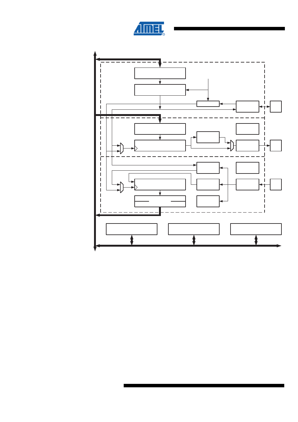
Figure 23-1. USART Block Diagram
(1)
PARITY
GENERATOR
UBRR [H:L]
UDR (Transmit)
UCSRA
UCSRB
UCSRC
BAUD RATE GENERATOR
TRANSMIT SHIFT REGISTER
RECEIVE SHIFT REGISTER
RxD
TxD
PIN
CONTROL
UDR (Receive)
PIN
CONTROL
XCK
DATA
RECOVERY
CLOCK
RECOVERY
PIN
CONTROL
TX
CONTROL
RX
CONTROL
PARITY
CHECKER
DATA BUS
OSC
SYNC LOGIC
Clock Generator
Transmitter
Receiver
Note:
1. See
and
for USART pin placement.
23.3 Clock Generation
The clock generation logic generates the base clock for the transmitter and receiver.
The USART supports four modes of clock operation: Normal asynchronous, double
speed asynchronous, master synchronous and slave synchronous mode. The UMSELn
bit in USART Control and Status Register C (UCSRnC) selects between asynchronous
and synchronous operation. Double speed (asynchronous mode only) is controlled by
the U2Xn found in the UCSRnA register. When using synchronous mode (UMSELn =
1), the data direction register for the XCKn pin (DDR_XCKn) controls whether the clock
source is internal (master mode) or external (slave mode). The XCKn pin is only active
when using synchronous mode.